Oxide-nitride-oxide stack having multiple oxynitride layers

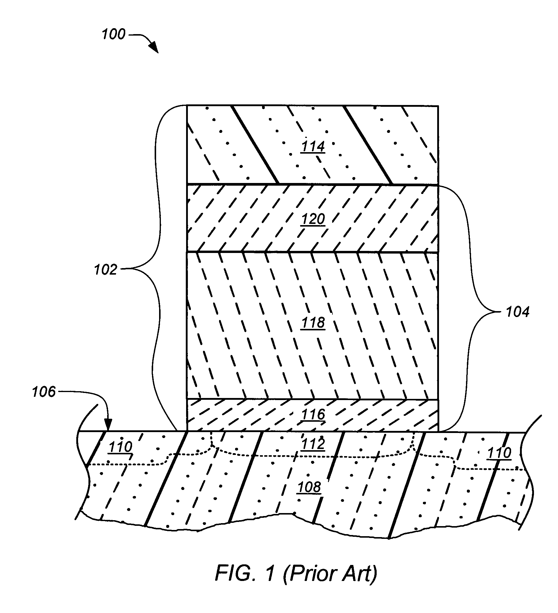
a technology of oxynitride and nitride, which is applied in the field of oxide-nitride-oxide stacks, can solve the problems of poor data retention of nitride or oxynitride layers, limited devices, and stochiometry of oxynitride layers 118/b> is neither uniform nor optimized across the thickness of layers

Inactive Publication Date: 2009-07-16
LONGITUDE FLASH MEMORY SOLUTIONS LTD
View PDF14 Cites 96 Cited by
  • Summary
  • Abstract
  • Description
  • Claims
  • Application Information

AI Technical Summary

Problems solved by technology

One problem with conventional SONOS structures 102 and methods of forming the same is the poor data retention of the nitride or oxynitride layer 118 that limits the device 100 lifetime and / or its use in several applications due to leakage current through the layer.
Another problem with conventional SONOS structures 102 and methods of forming the same is the stochiometry of the oxynitride layer 118 is neither uniform nor optimized across the thickness of the layer.
Consequently, the charge storage characteristics, and in particular programming and erase speed and data retention of a memory device 100 made with the ONO stack 104, are adversely effected.

Method used


Image

  • Oxide-nitride-oxide stack having multiple oxynitride layers
  • Oxide-nitride-oxide stack having multiple oxynitride layers
  • Oxide-nitride-oxide stack having multiple oxynitride layers

Examples


Embodiment Construction

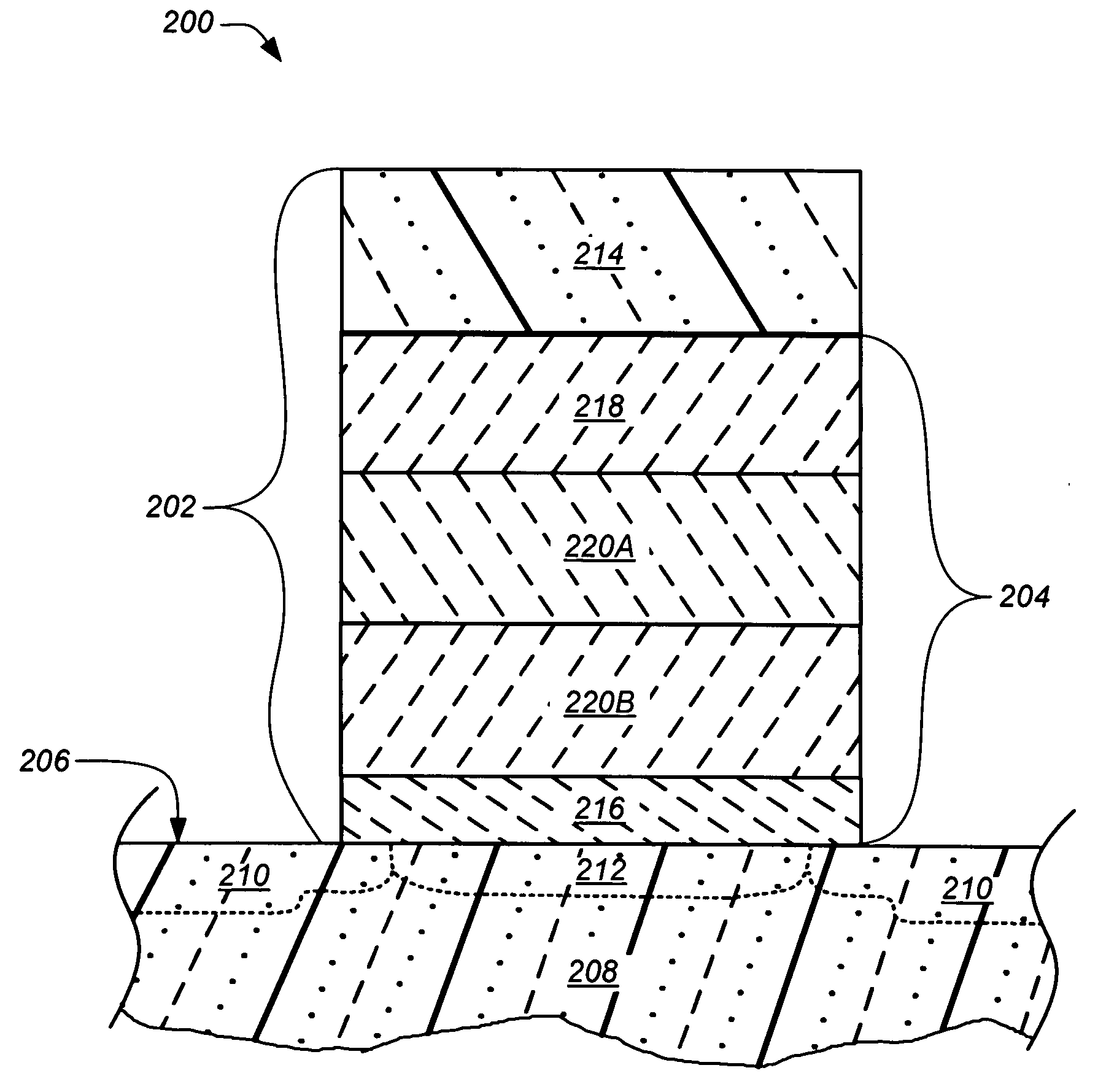
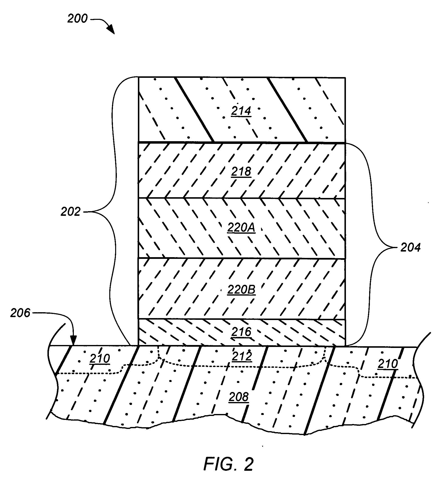
[0015]The present invention is directed generally to an oxide-nitride-oxide (ONO) structure including a multi-layer charge storing layer and methods for making the same. The ONO structure and method are particularly useful for forming a memory layer in a memory device, such as a silicon-oxide-nitride-oxide-silicon (SONOS) memory transistor.

[0016]In the following description, for purposes of explanation, numerous specific details are set forth in order to provide a thorough understanding of the present invention. It will be evident, however, to one skilled in the art that the present invention may be practiced without these specific details. In other instances, well-known structures, and techniques are not shown in detail or are shown in block diagram form in order to avoid unnecessarily obscuring an understanding of this description.

[0017]Reference in the description to “one embodiment” or “an embodiment” means that a particular feature, structure, or characteristic described in con...


PUM

PropertyMeasurementUnit
temperatureaaaaaaaaaa
operating temperatureaaaaaaaaaa
temperatureaaaaaaaaaa

Abstract

A semiconductor device including an oxide-nitride-oxide (ONO) structure having a multi-layer charge storing layer and methods of forming the same are provided. Generally, the method involves: (i) forming a first oxide layer of the ONO structure; (ii) forming a multi-layer charge storing layer comprising nitride on a surface of the first oxide layer; and (iii) forming a second oxide layer of the ONO structure on a surface of the multi-layer charge storing layer. Preferably, the charge storing layer comprises at least two silicon oxynitride layers having differing stoichiometric compositions of Oxygen, Nitrogen and / or Silicon. More preferably, the ONO structure is part of a silicon-oxide-nitride-oxide-silicon (SONOS) structure and the semiconductor device is a SONOS memory transistor. Other embodiments are also disclosed.

Description

CROSS-REFERENCE TO RELATED APPLICATIONS[0001]The present application claims the benefit of priority under 35 U.S.C. 119(e) to U.S. Provisional Patent Application Ser. No. 60 / 931,947, entitled Oxide-Nitride-Oxide Stack Having Multiple Oxynitride Layers; which application is hereby incorporated by reference.TECHNICAL FIELD[0002]This invention relates to semiconductor processing and, more particularly to an oxide-nitride-oxide stack having an improved oxide-nitride or oxynitride layer and methods of forming the same.BACKGROUND OF THE INVENTION[0003]Non-volatile semiconductor memories, such as a split gate flash memory, typically use a stacked floating gate type field effect transistors, in which electrons are induced into a floating gate of a memory cell to be programmed by biasing a control gate and grounding a body region of a substrate on which the memory cell is formed.[0004]An oxide-nitride-oxide (ONO) stack is used as either a charge storing layer, as in silicon-oxide-nitride-oxi...

Claims


Application Information

Patent Timeline
Patent Type & Authority Applications(United States)
IPC IPC(8): H01L29/792H01L21/336
CPCC23C16/0272C23C16/308G11C16/0466H01L29/792H01L21/3145H01L29/7833H01L21/28282H01L29/518H01L29/40117H01L21/02148H01L21/0214H01L21/02164H01L21/022H01L21/02238H01L21/02271H01L21/02211H01L21/02255H10B43/30
Inventor LEVY, SAGYRAMKUMAR, KRISHNASWAMYJENNE, FREDRICKGEHA, SAM
Owner LONGITUDE FLASH MEMORY SOLUTIONS LTD
Why Eureka
Try Eureka