Packaging structure, method for manufacturing the same, and method for using the same

a packaging structure and manufacturing method technology, applied in the direction of semiconductor devices, electrical devices, semiconductor/solid-state device details, etc., can solve the problems of time and cost of the packaging process, and the conventional packaging structure often has some disadvantages, so as to improve the packaging efficiency

Inactive Publication Date: 2009-07-16
ANHUI HAIHUA CHEM
View PDF1 Cites 3 Cited by
  • Summary
  • Abstract
  • Description
  • Claims
  • Application Information

AI Technical Summary

Benefits of technology

[0014]Depending on the present invention, the packaging structure with a pre-cured layer is thus provided for miniaturized electrical device. Furthermore, the packaging efficiency is improved.

Problems solved by technology

However, the conventional packaging structure often has some disadvantages.
Therefore, the time and cost of the packaging process are magnified.

Method used


Image

  • Packaging structure, method for manufacturing the same, and method for using the same
  • Packaging structure, method for manufacturing the same, and method for using the same
  • Packaging structure, method for manufacturing the same, and method for using the same

Examples


Embodiment Construction

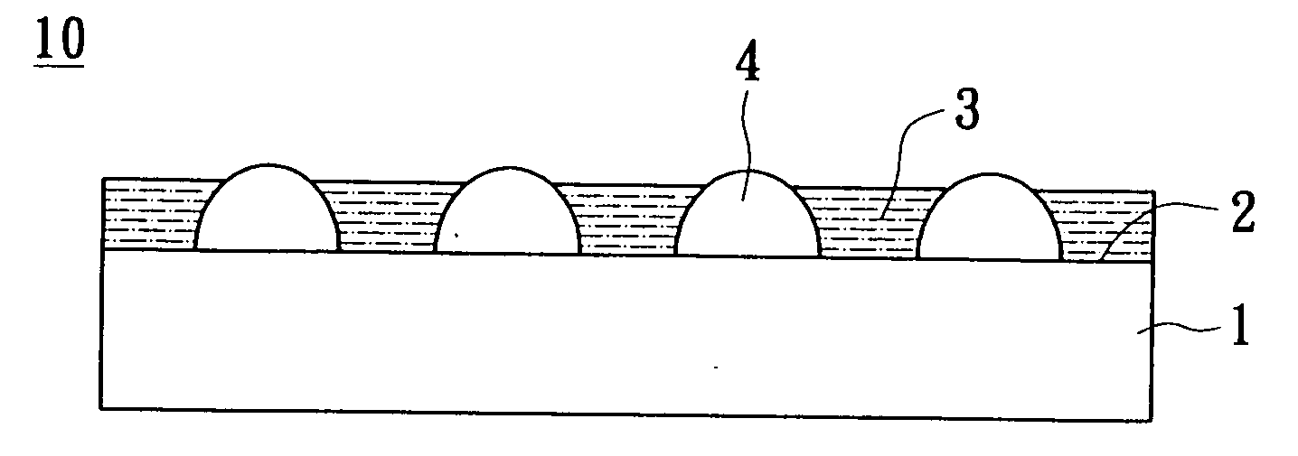
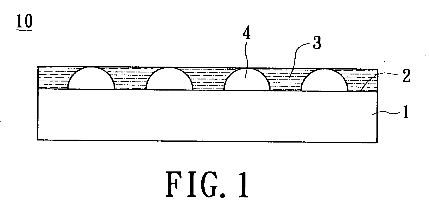
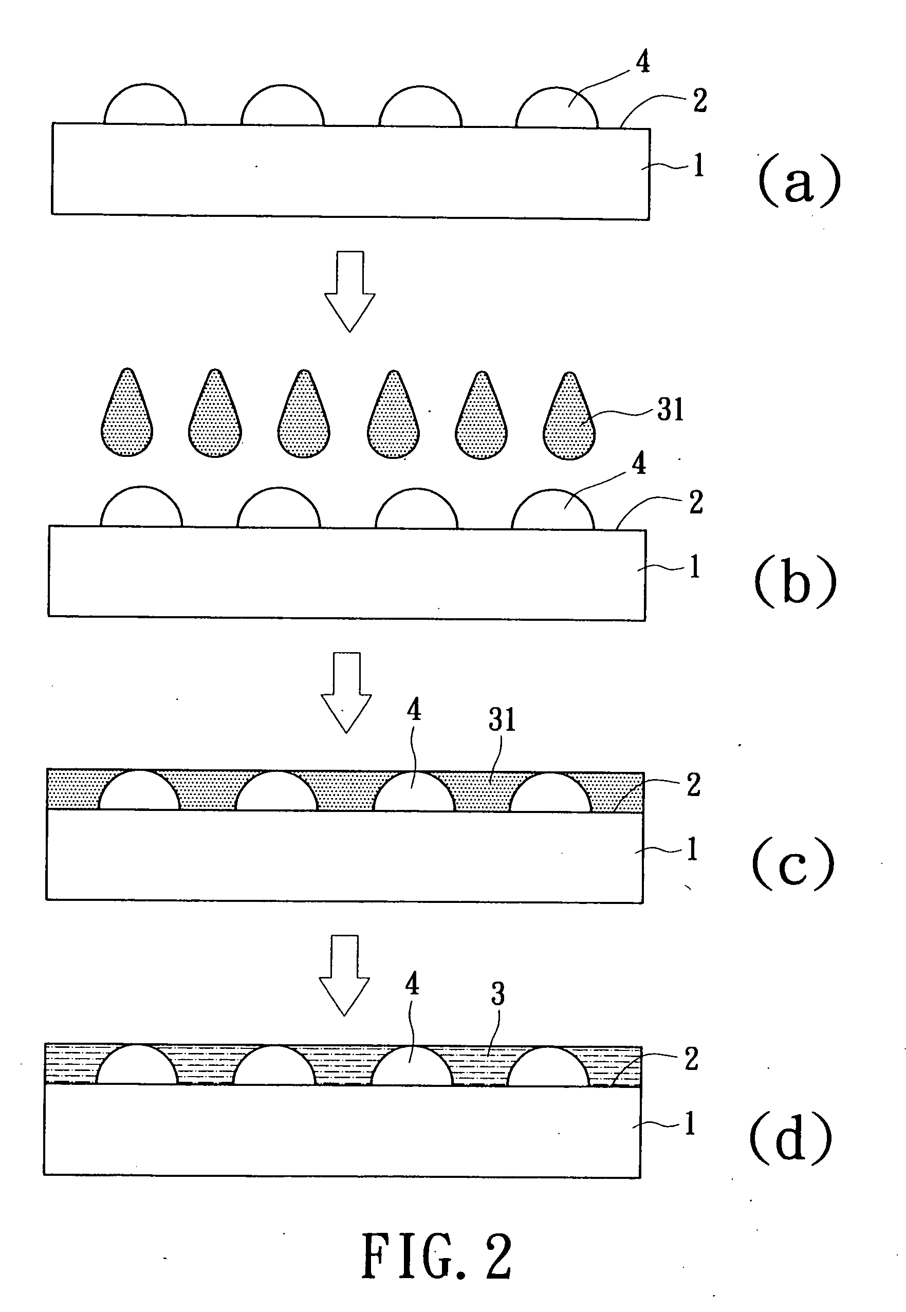
[0021]Please refer to FIG. 1, the invention discloses a packaging structure 10 which is applied to a surface mounting technology (SMT) process. The packaging structure 10 comprises a chip module 1 having a package surface 2 and a pre-cured layer 3 formed on the packaging surface 2 of the chip module 1. The chip module 1 can be an IC chip or another electronic module for connecting on the substrate 5 (shown in FIG. 4). The package surface 2 has a plurality of connecting protrusions 4 and the connecting protrusions are metallic protrusions, solder balls, or another connecting means familiar with the skilled person. The pre-cured layer 3 is formed by pre-curing a gluing material 31 (shown in FIG. 2). The gluing material 31 has thermal-forming property and pre-cures at a predetermined temperature. In the embodiment, the gluing material 31 pre-cures at a predetermined temperature higher than room temperature on the package surface 2. Preferably, the gluing material 31 is disposed between...


PUM


Abstract

A packaging structure applied for a surface mounting process, comprising: a chip module having a packaging surface; and a pre-cured layer formed on the packaging surface of the chip module. As above-mentioned, the structure is employed for protecting the external surface of the wafer. The pre-cured layer is formed on pre-curing a gluing material and the gluing material is uniformly filled with the space between the connecting protrusions on the packaging surface. The pre-cured later is post-curing in a connecting process for mounting the connecting protrusions to the substrate so that the connecting strength is improved. Moreover, the rate of the packaging process is increasing.

Description

BACKGROUND OF THE INVENTION[0001]1. Field of the Invention[0002]The present invention relates to a packaging structure and a method for manufacturing and using the same, and in particular to a packaging structure having a pre-cured layer thereon and a method for manufacturing and using the same.[0003]2. Description of Related Art[0004]As the development of the semiconductor advances, the functions of semiconductor chips become more and more powerful. Due to ever larger data transmission of semiconductor chips, the pins of the chips are increasing. Thus, the packaging technology to protect the chips and delicate chip pins have a direct impact on improving the industry.[0005]Packaging plays an important role for protecting the chip or IC circuit from humidity or collision. Now packaging has to dissipate heat from the chip so as to maintain the environment of the chip in a suitable condition for operation.[0006]However, the conventional packaging structure often has some disadvantages....

Claims


Application Information

Patent Timeline
Patent Type & Authority Applications(United States)
IPC IPC(8): H01L23/488H01L21/58
CPCH01L21/563H01L24/27H01L2224/16H01L2224/73203H01L2224/83191H01L2224/83856H01L2224/73204H01L2924/01027H01L2924/14H01L2924/01006H01L2924/01033H01L24/29H01L2924/01005H01L2224/73104
Inventor HUANG, CHUNG-ERLIAO, CHIH-HAO
Owner ANHUI HAIHUA CHEM
Why Eureka
Try Eureka