Method to recover underfilled modules by selective removal of discrete components

a discrete component and module technology, applied in the field of electronic devices, can solve the problems of rework of lead free alloy containing assemblies, adversely affecting the performance of packages, irreparable damage to adjacent components, etc., and achieves the effect of easy transfer of an array of solder bumps and little damag

Inactive Publication Date: 2009-07-23
GLOBALFOUNDRIES INC
View PDF2 Cites 33 Cited by
  • Summary
  • Abstract
  • Description
  • Claims
  • Application Information

AI Technical Summary

Benefits of technology

[0019]The perforated underfill matrix is then preferably removed using a dry blasting process, such as, by using a mild abrasive material such as sodium bicarbonate which is projected against the perforated underfill matrix using a compressed gas directed through a nozzle. The gas-entrained abrasive abrasively removes the underfill matrix from the surface of the substrate with little damage to the substrate surface. The abrasive also cleans the surfaces of the metallization pads preparing them for subsequent solder attach.
[0020]Further, in accordance with the invention, new solder may be transferred onto the exposed surface pads of the substrate by providing a blank chip having a release layer on a surface thereof for easily transferring an array of solder bumps applied onto said surface. An array of solder bumps is deposited on the release layer in a pattern corresponding to the pattern of the connections of the die. The array of solder connections are then aligned with and applied to the site that is to be reworked. The module and blank chip assembly are heated to reflow and transfer the solder connections from the blank onto the solder pads on the substrate. The blank may then be removed from the module allowing visual inspection and confirmation of the solder transfer onto every connection on the substrate.

Problems solved by technology

These solder bumps are then underfilled (or encapsulated) to protect them from moisture, mobile ions, corrosives (e.g., acidic or alkaline species) and separation of the solder bump electrical connections, all of which will adversely affect the performance of the package.
After forming the solder bumps between the chip(s) and substrate, testing one or more of these chips may show them to be defective.
This can occur due to incomplete initial test coverage or the inability to drive all circuits under highly stressful thermal environments, which are difficult to create without underfilling the die.
When a module with underfill residing between the chip and substrate is found to have a defective die this presents a number of problems in the rework process since the underfill material is generally a very durable material by design.
However, the higher rework temperatures can irreparably damage adjacent components on an organic or ceramic board, and as such, rework of lead free alloy containing assemblies has become a critical issue in the qualification of this technology.

Method used


Image

  • Method to recover underfilled modules by selective removal of discrete components
  • Method to recover underfilled modules by selective removal of discrete components
  • Method to recover underfilled modules by selective removal of discrete components

Examples


Embodiment Construction

)

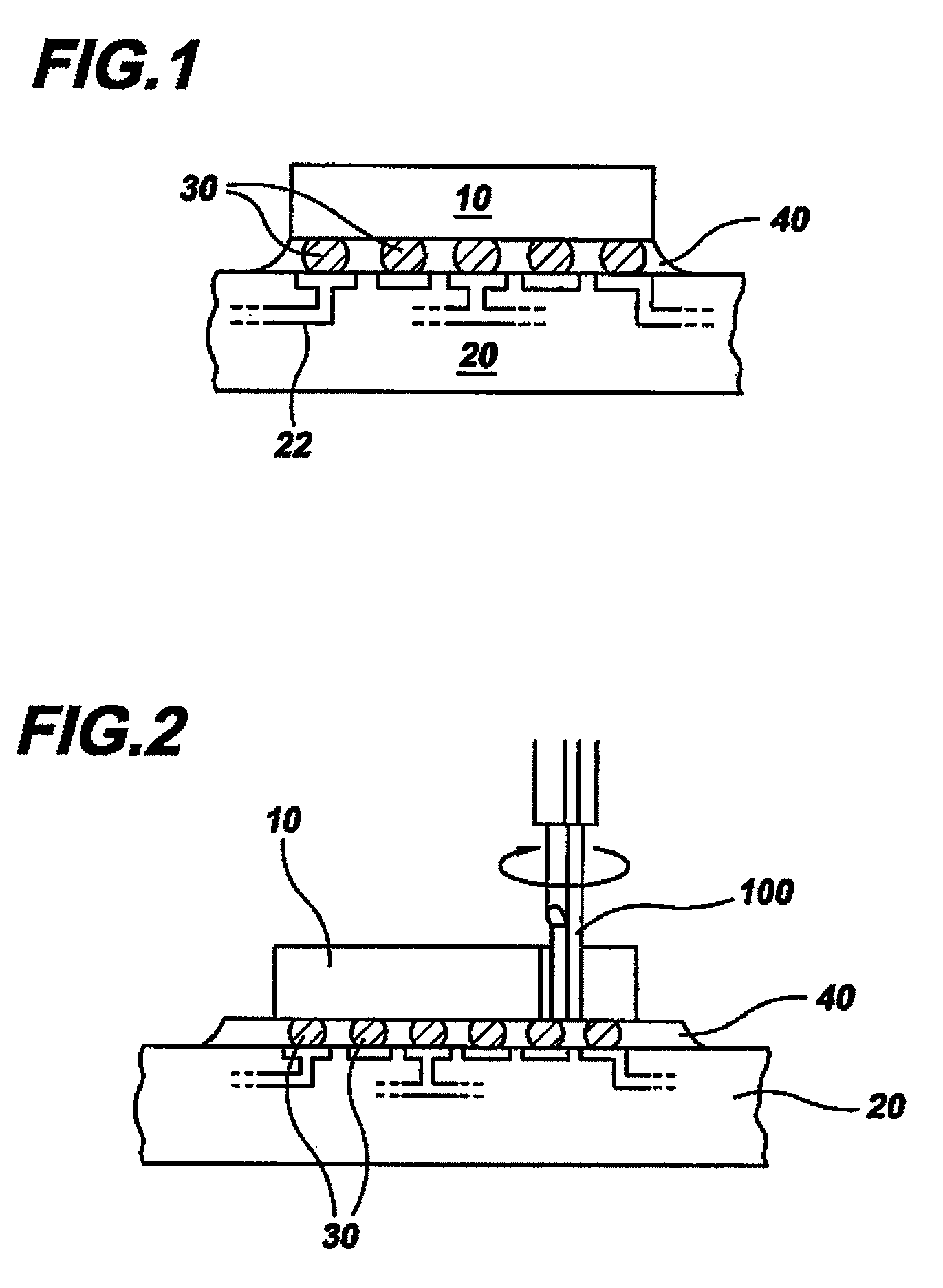
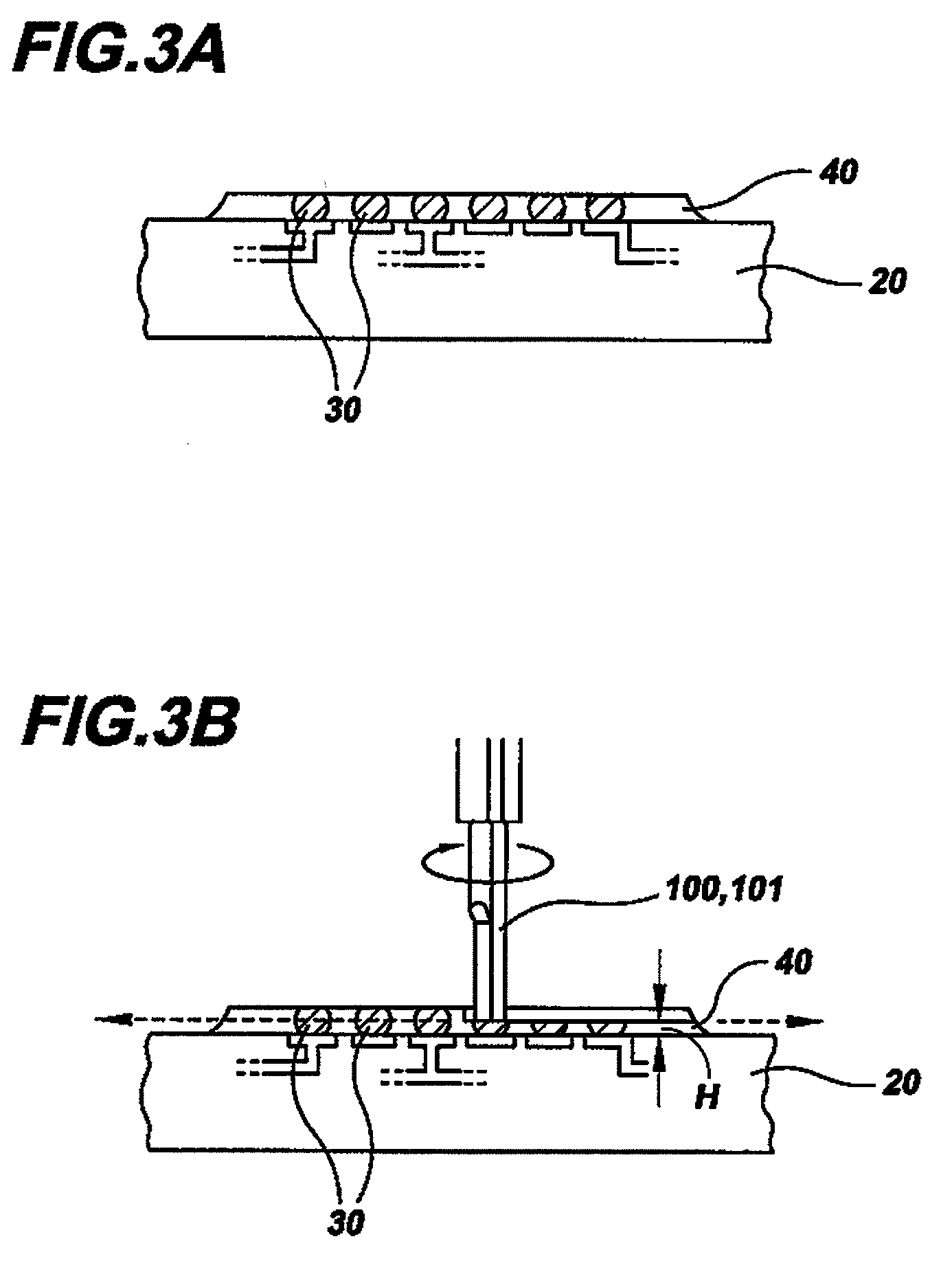
[0039]In describing the preferred embodiment of the present invention, reference will be made herein to FIGS. 1-9C of the drawings in which like numerals refer to like features of the invention.

[0040]The material set and method disclosed herein are the basis for a low cost electronic package rework process including appropriate hardware and equipment alternatives. An advantage of the foregoing rework method and material set is that it can be implemented on many levels of scale at minimal cost, with minimal effort and ease of flexibility, as well as across a variety of differing types and material sets of electronic packages.

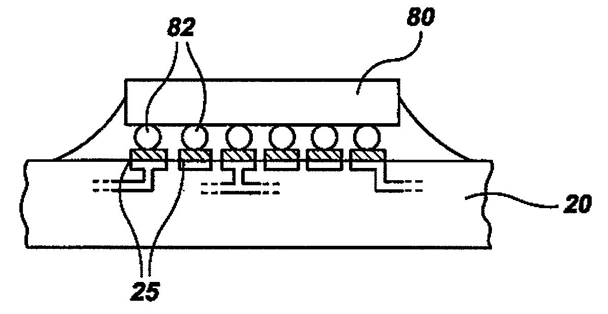
[0041]In accordance with the invention, an electronic package typically has many electrical components attached to a substrate using encapsulated solder connections. Referring to FIG. 1, for ease of understanding the invention, reference is made to the electronic device or component being removed from the module as a semiconductor chip or die 10 attached to a su...


PUM

PropertyMeasurementUnit
heightsaaaaaaaaaa
heightsaaaaaaaaaa
melting pointaaaaaaaaaa

Abstract

Methods and reworked intermediate and resultant electronic modules made thereby, whereby a component in need of rework is located and removed from the module to reveal encapsulated solder connections residing within an underfill matrix. Heights of both the solder connections and underfill matrix are reduced, followed by etching the solder out of the solder connections to form openings within the underfill matrix. The underfill material is then removed to expose metallurgy of the substrate. A blank having a release layer with an array of solder connections is aligned with the exposed metallurgy, and this solder array is transferred from the blank onto the metallurgy. The transferred solder connections are then flattened using heat and pressure, followed by attaching solder connections of a new component to the flattened solder connections and underfilling these reworked solder connections residing between the new chip and substrate.

Description

BACKGROUND OF THE INVENTION[0001]1. Field of the Invention[0002]The present invention relates to electronic devices, and in particular, to removing and reworking underfilled integrated circuit chips on an electronic module.[0003]2. Description of Related Art[0004]Electronic components include both Single Chip Modules (SCMs) and Multi Chip Modules (MCMs). While SCMs contain a single chip, MCMs contain numerous chips on a substrate, and as such, are key components for many high-end computer servers and mainframes.[0005]Often, the electronic components in SCMs and MCMs are joined to other components by solder interconnections whereby these solder interconnections are made by soldering pads on a surface of a first of these electronic components to corresponding soldering pads on the surface of the second component. Typical solder surface mount processes involve screening solder paste onto exposed metallic pads of a board or substrate, followed by a thermal reflow to bring the solder int...

Claims


Application Information

Patent Timeline
Patent Type & Authority Applications(United States)
IPC IPC(8): H01L21/70H01L23/02
CPCH01L21/56H01L21/563H01L2924/01327H01L2924/01322H01L2224/73204H01L2224/32225H01L2224/16225H01L2224/73203H01L2924/01078H01L2924/09701H05K3/225H05K3/3436H05K2203/0278H05K2203/0338H05K2203/176H01L2924/00H01L24/98Y02P70/50
Inventor ARVIN, CHARLES L.FASANO, BENJAMIN V.INTERRANTE, MARIO J.POMERANTZ, GLENN A.
Owner GLOBALFOUNDRIES INC
Why Eureka
Try Eureka