Solid-state imaging device, method of fabricating solid-state imaging device, and camera

a solid-state imaging and imaging device technology, applied in the direction of semiconductor/solid-state device details, radio frequency controlled devices, television systems, etc., can solve the problems of insufficient cover of the pad portion, insufficient reliability, and insufficient interlayer dielectric b>61/b> that is exposed from the opening, etc., to achieve the effect of improving the product reliability of the solid-state imaging devi

Active Publication Date: 2009-07-23
SONY SEMICON SOLUTIONS CORP
View PDF7 Cites 77 Cited by
  • Summary
  • Abstract
  • Description
  • Claims
  • Application Information

AI Technical Summary

Benefits of technology

[0019]In an embodiment of the invention, the insulating film is extendedly formed from the surface of the semiconductor layer to the internal side-wall of the opening of the pad portion formed on the solid state imaging device to insulate the semiconductor layer, advert effect on the semiconductor layer and the plurality of wiring layers may be prevented.
[0020]According to an embodiment of the invention, since the insulating film is extendedly coated from the surface of the semiconductor layer to the internal side-wall of the opening of the pad portion, the advert effect on the semiconductor layer and the plurality of wiring layers may be prevented, thereby improving product reliability of the solid-state imaging device.

Problems solved by technology

Thus, only providing the interlayer dielectric 61 that is exposed from the opening 62 may not be sufficient to prevent the interconnects 52 from absorbing moisture.
Moreover, the pad portion may be coated with an organic film, however, the organic film may not be able to cover the pad portion sufficiently (not enough coverage), thereby exhibiting not enough reliability.
Further, since the related art shield film used in the backside-illuminated solid-state imaging device is electrically floating, electrical potential is not stabilized.
As a result, the electrical potential of the shield film may cause an adverse effect on pixels of the solid-state imaging device.

Method used


Image

  • Solid-state imaging device, method of fabricating solid-state imaging device, and camera
  • Solid-state imaging device, method of fabricating solid-state imaging device, and camera
  • Solid-state imaging device, method of fabricating solid-state imaging device, and camera

Examples


first embodiment

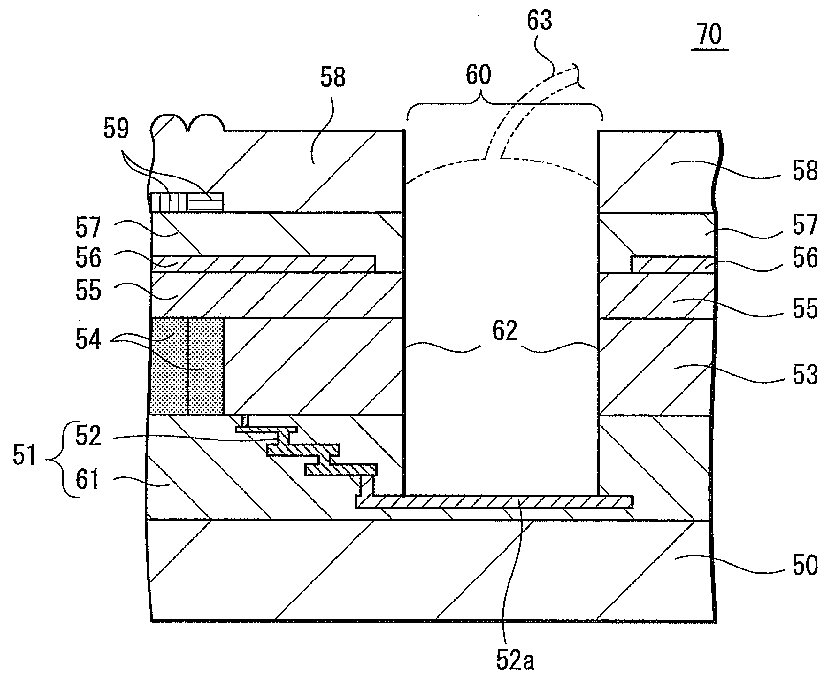
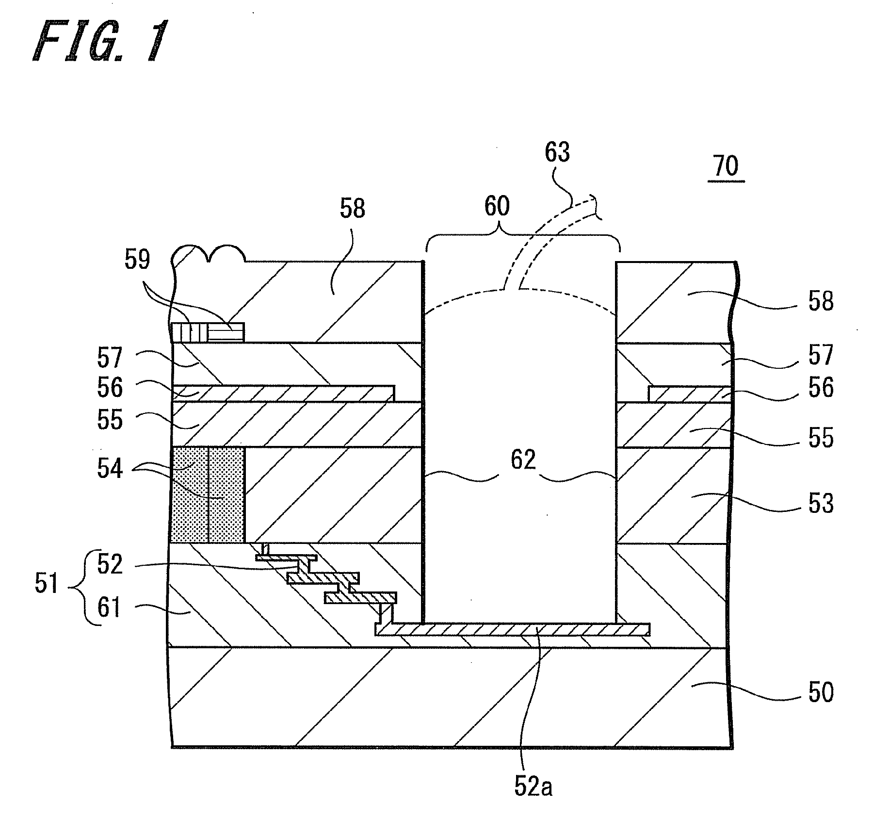
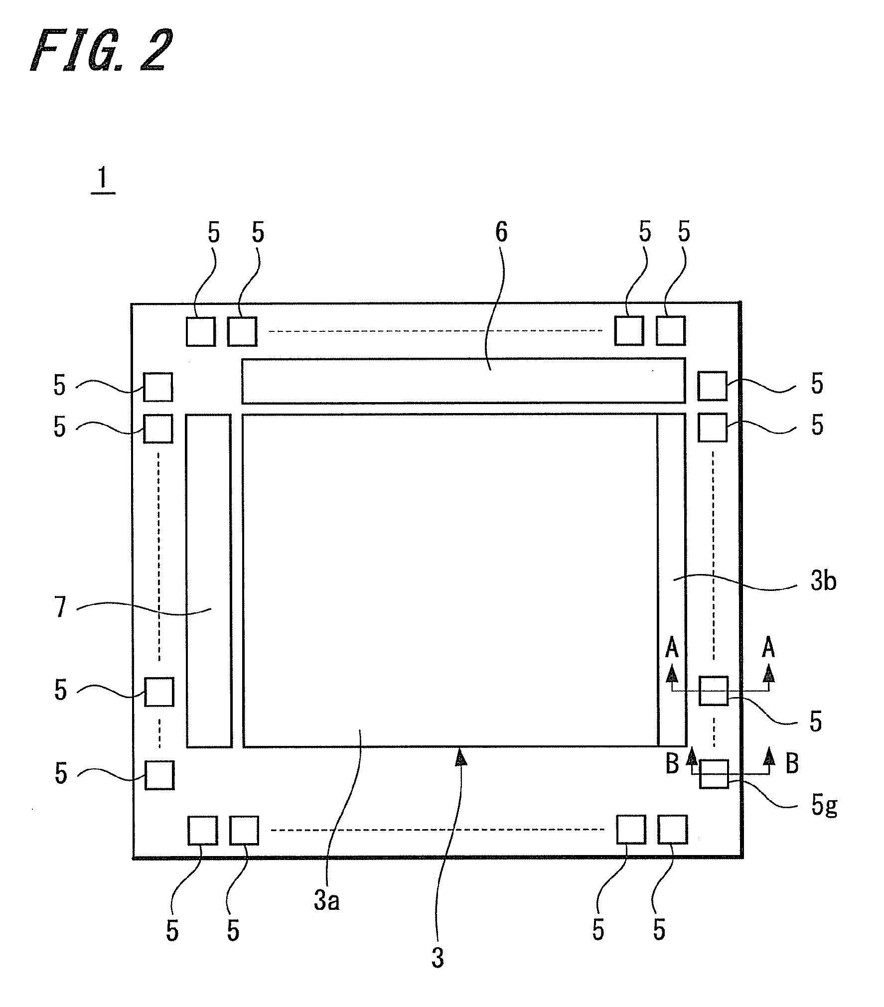
[0040]FIG. 2 is a schematic diagram illustrating a solid-state imaging device according to the invention. A solid-state imaging device according to embodiments of the invention is a backside-illuminated CMOS solid-state imaging device.

[0041]A solid-state imaging device according to an embodiment of the invention is configured to include imaging region 3, peripheral circuitries 6, 7, pad portions 5.

[0042]The imaging region 3 includes a matrix of numerous unit pixels, and address lines arranged in rows, and signal lines arranged in columns. The imaging region 3 includes an effective pixel region 3a and an optical black region 3b that determines a black level of each pixel.

[0043]The optical black region 3b also includes similar pixels as those included in the effective pixel region 3a. The pixels in the optical black region 3b are arranged outside of the effective pixel region 3a. An entire region of the solid-state imaging device, excluding the photoelectric converters (light-receivin...

second embodiment

[0079]Next, FIG. 17 is a schematic diagram illustrating a solid-state imaging device according to the invention. The solid-state imaging device according to this embodiment, aluminum is used as a material of the shield film, and the same reference numerals as those used in FIGS. 4, 5 are used to denote the corresponding parts in FIGS. 17A, 17B, and duplicated descriptions thereof are thus omitted.

[0080]The solid-state imaging device according to the second embodiment includes the same configuration as that shown in FIG. 1. FIG. 17A shows the A-A cross-sectional configuration while FIG. 17B shows the B-B cross-sectional configuration in FIG. 2.

[0081]The solid-state imaging device according to the second embodiment is manufactured in compliance with the fabricating steps for the first embodiment; however, the location of depositing a shield film 22 in the second embodiment is different from that shown in the first embodiment.

[0082]In the second embodiment, an area of the shield film 2...


PUM


Abstract

Disclosed is a solid-state imaging device receiving incident light from a backside thereof. The imaging device includes a semiconductor layer on which a plurality of pixels including photoelectric converters and pixel transistors are formed, a wiring layer formed on a first surface of the semiconductor layer, a pad portion formed on a second surface of the semiconductor layer, an opening formed to reach a conductive layer of the wiring layer, and an insulating film extendedly coated from the second surface to an internal side-wall of the opening so as to insulate the semiconductor layer.

Description

CROSS REFERENCES TO RELATED APPLICATIONS[0001]The present invention contains subject matter related to Japanese Patent Application JP 2008-010904 filed in the Japanese Patent Office on Jan. 21, 2008, the entire contents of which being incorporated herein by reference.BACKGROUND OF THE INVENTION[0002]1. Field of the Invention[0003]The invention relates to a backside-illuminated solid-state imaging device, a method of fabricating the backside-illuminated solid-state imaging device, and a camera.[0004]2. Description of the Related Art[0005]In a CMOS type solid-state imaging device, there has been disclosed a backside-illuminated solid-state imaging device for improving photoelectric conversion efficiency and sensitivity to incident light. In the backside-illuminated solid-state imaging device, light is illuminated from backside of the solid-state imaging device. The backside-illuminated solid-state imaging device is configured to include a semiconductor substrate on which photodiodes a...

Claims


Application Information

Patent Timeline
Patent Type & Authority Applications(United States)
IPC IPC(8): H04N5/335H01L31/02H01L21/30H01L27/14H01L27/146H04N5/357H04N5/369H04N5/374
CPCH01L27/14623H01L27/14632H01L27/14687H01L27/1464H01L27/14636H01L21/76898H01L23/481H01L2224/48451H01L24/48H01L2224/48463H01L24/45H01L2224/45144H01L2224/02166H01L2924/00014H01L27/146
Inventor AKIYAMA, KENTARO
Owner SONY SEMICON SOLUTIONS CORP
Why Eureka
Try Eureka