
Common test logic for multiple operation modes

a test logic and operation mode technology, applied in the direction of detecting faulty computer hardware, error detection/correction, instruments, etc., can solve the problems of increasing complexity of additional circuits, consuming chip area and power consumption

Inactive Publication Date: 2009-07-23
INTEL CORP
View PDF6 Cites 11 Cited by
  • Summary
  • Abstract
  • Description
  • Claims
  • Application Information

AI Technical Summary

Problems solved by technology

However, additional circuits increase complexity consume chip area and power consumption.

Method used


Image

  • Common test logic for multiple operation modes
  • Common test logic for multiple operation modes
  • Common test logic for multiple operation modes

Examples


Embodiment Construction

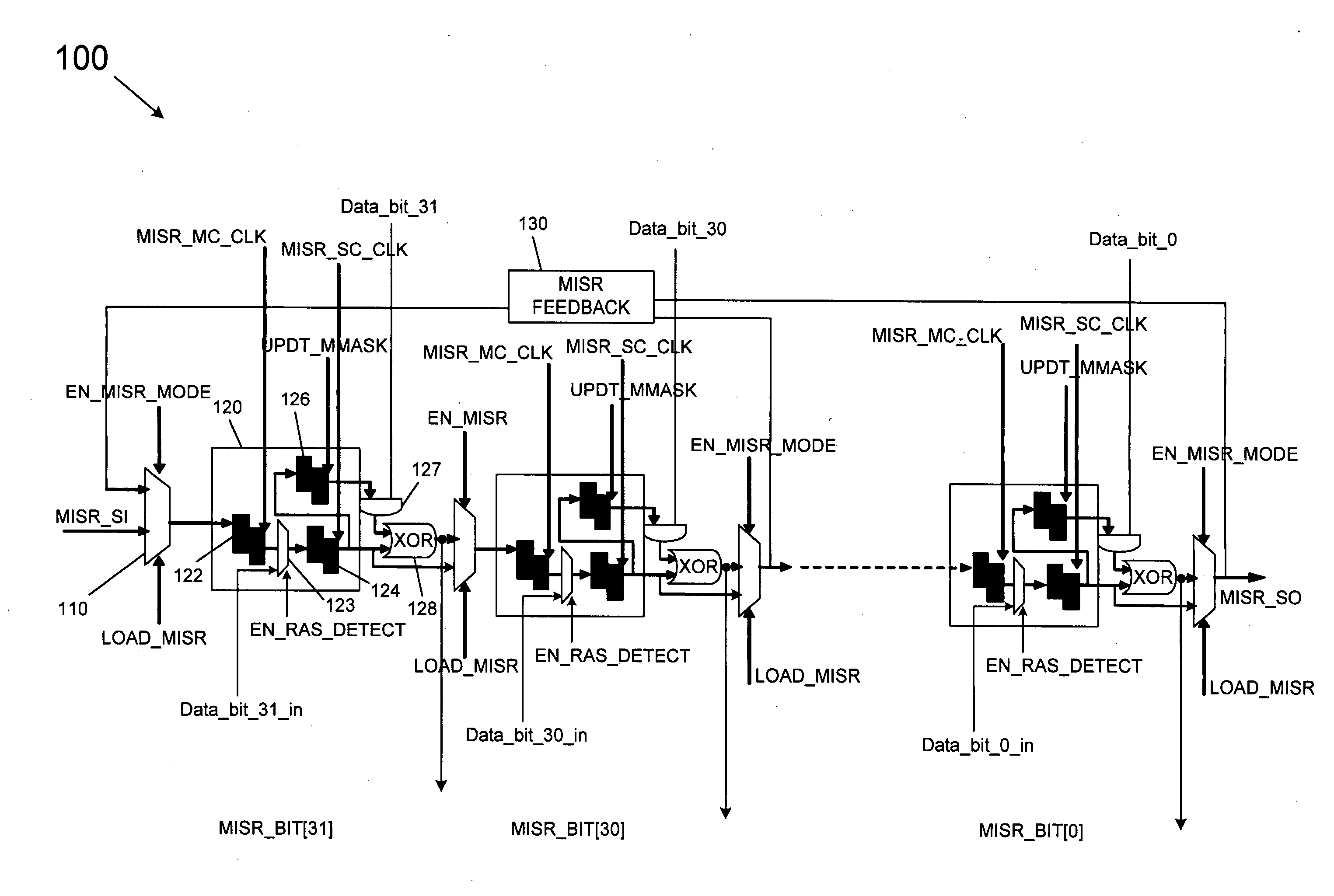
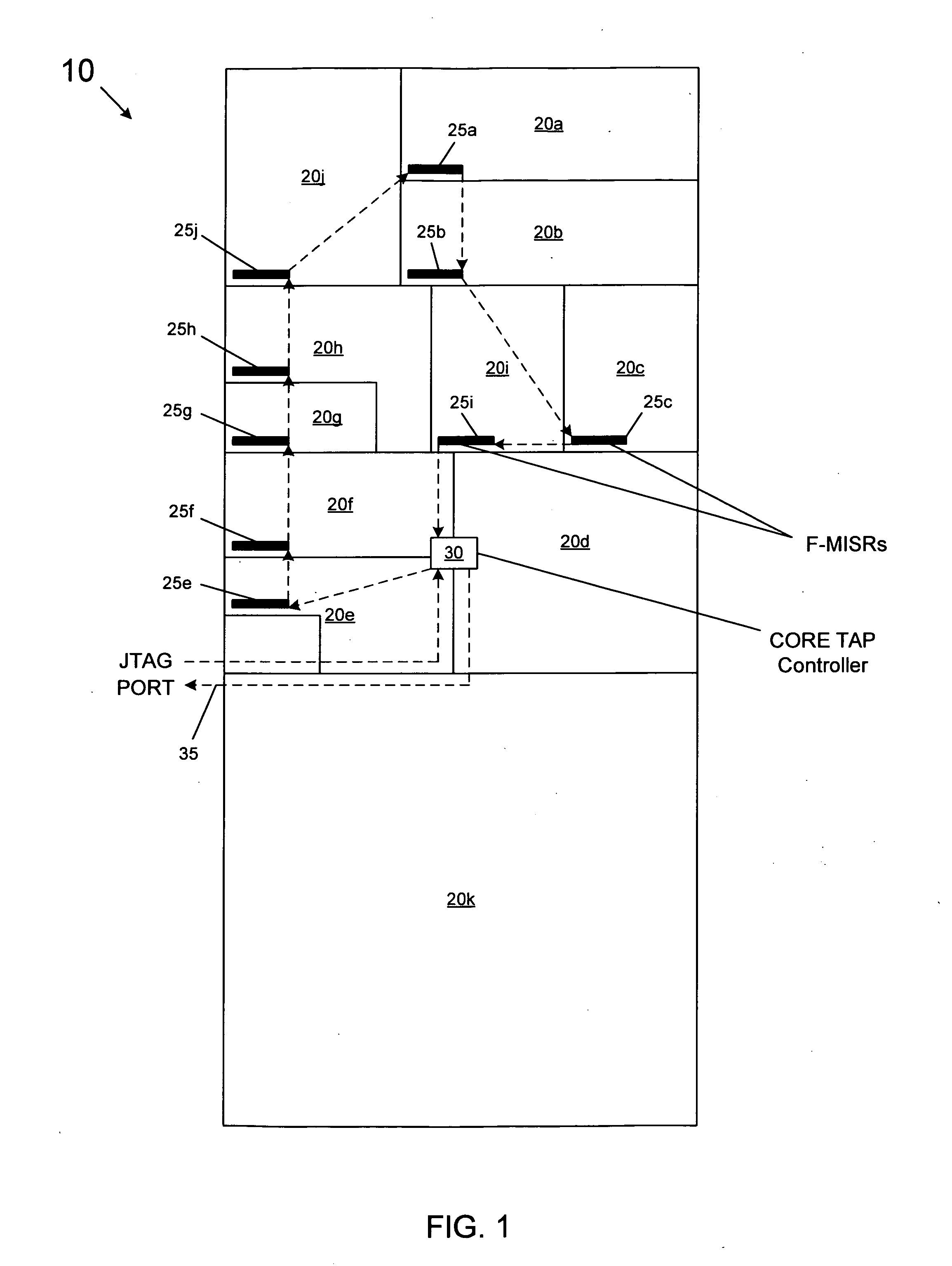
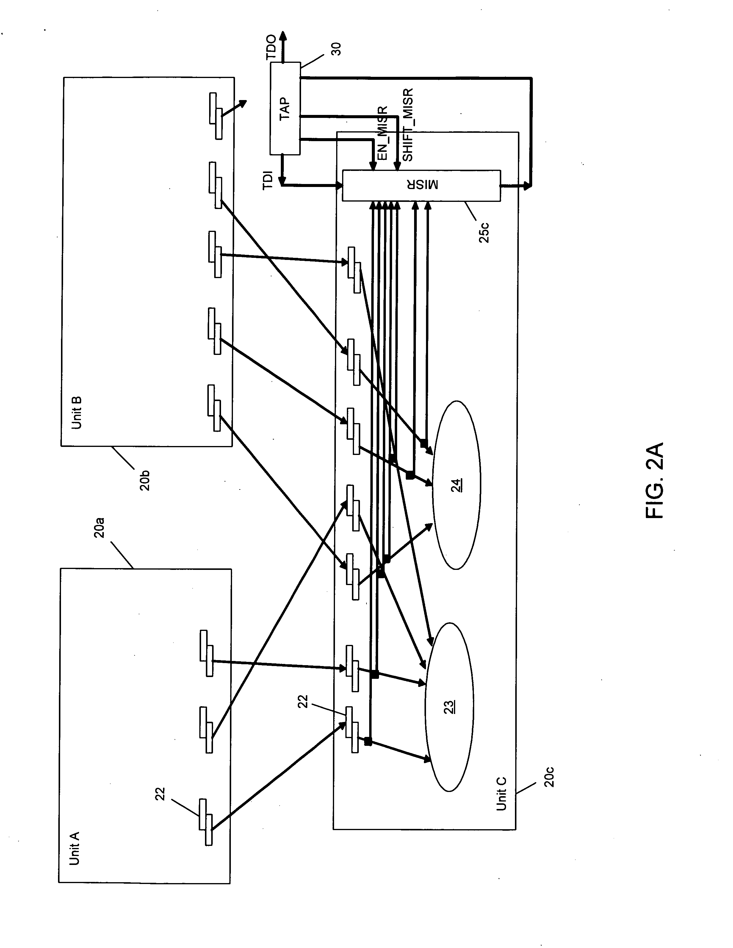
[0010]Embodiments may provide an apparatus and a structure to enable design for test (DFT), reliability-availability-serviceability (RAS), debug and test features all to be supported through a common logic structure embedded in a processor core. That is, generic, common test circuitry in accordance with an embodiment of the present invention can be used to handle test operations occurring during design, debug, manufacturing testing, as well as during normal operation of the semiconductor device in the field. As examples, DFT operations may be used to test the device on prototype production. Functional test features may be tested by the same common circuitry during manufacture, for example, to speed bin different devices according to highest operating frequency. Still further, the same common circuitry can be used during RAS operations during normal operation of the device, such as for detection of soft errors, intermittent errors or errors due to voltage or power droops, or the like...


PUM


Abstract

In one embodiment, the present invention includes a processor having a plurality of logical units to perform operations on data. Each unit may include a multiple input shift register (MISR) at an input of the logical unit to collect and compress data from input signals to the unit. In turn, each MISR may includes bit cells, each having a first cell to receive incoming data and controlled by a first clock signal, a second cell to receive an output of the first cell and controlled by a second clock signal, a mask cell to receive an output of the second cell and to generate a mask signal responsive to a mask clock signal, and a multiplexer coupled between the first and second cells. Other embodiments are described and claimed.

Description

BACKGROUND[0001]Given the ever-increasing complexity of semiconductor devices, many integrated circuits (ICs) are designed with various test circuitry present. Typically, such test circuitry is specialized to perform a particular test on a given functional unit or block of the semiconductor device. For example, such test circuits can include design for test (DFT) circuits and other circuitry used for debug or test features. Still further, some circuits include additional error detection and / or correction circuitry such as may be used during operation modes in the field when high levels of reliability-availability-serviceability (RAS) are needed.[0002]However, additional circuits increase complexity consume chip area and power consumption. Furthermore, significant design efforts are needed to develop specialized circuitry for such diverse needs.BRIEF DESCRIPTION OF THE DRAWINGS[0003]FIG. 1 is a block diagram of a semiconductor device in accordance with one embodiment of the present i...

Claims


Application Information

Patent Timeline
Patent Type & Authority Applications(United States)
IPC IPC(8): G01R31/3177G06F11/25
CPCG01R31/318547G06F11/2236G01R31/31858
Inventor JABER, TALALWU, DAVID M.ZHANG, MING
Owner INTEL CORP
Learn More