Method of Manufacturing a Coil Inductor

a coil inductor and manufacturing method technology, applied in the field of coil inductor, can solve the problems of reducing the q of the inductor, wasting power dissipation of the substrate, and eddy current as a waste of power dissipation in the substrate, so as to reduce the eddy current

Active Publication Date: 2009-07-30
TAIWAN SEMICON MFG CO LTD
View PDF8 Cites 49 Cited by
  • Summary
  • Abstract
  • Description
  • Claims
  • Application Information

AI Technical Summary

Benefits of technology

[0007]The present invention is directed to a method of manufacturing a coil inductor, that it satisfies this need of reducing Eddy current generated by the inductor in the silicon substrate.

Problems solved by technology

Eddy current can be viewed as wasted power dissipation in the substrate.
This creates an energy loss to the inductor, which then lowers the Q of the inductor degrading its performance.
Therefore, when more power loss is generated by the Eddy current, the more it reduces the Q. Thus, a design challenge for inductors manufactured on silicon substrates has often been of how to reduce the generation of Eddy current.

Method used


Image

  • Method of Manufacturing a Coil Inductor
  • Method of Manufacturing a Coil Inductor
  • Method of Manufacturing a Coil Inductor

Examples


first embodiment

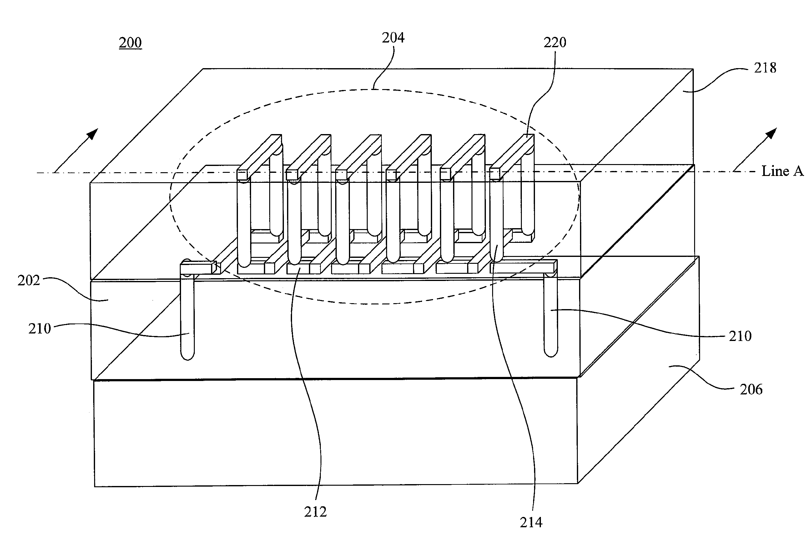
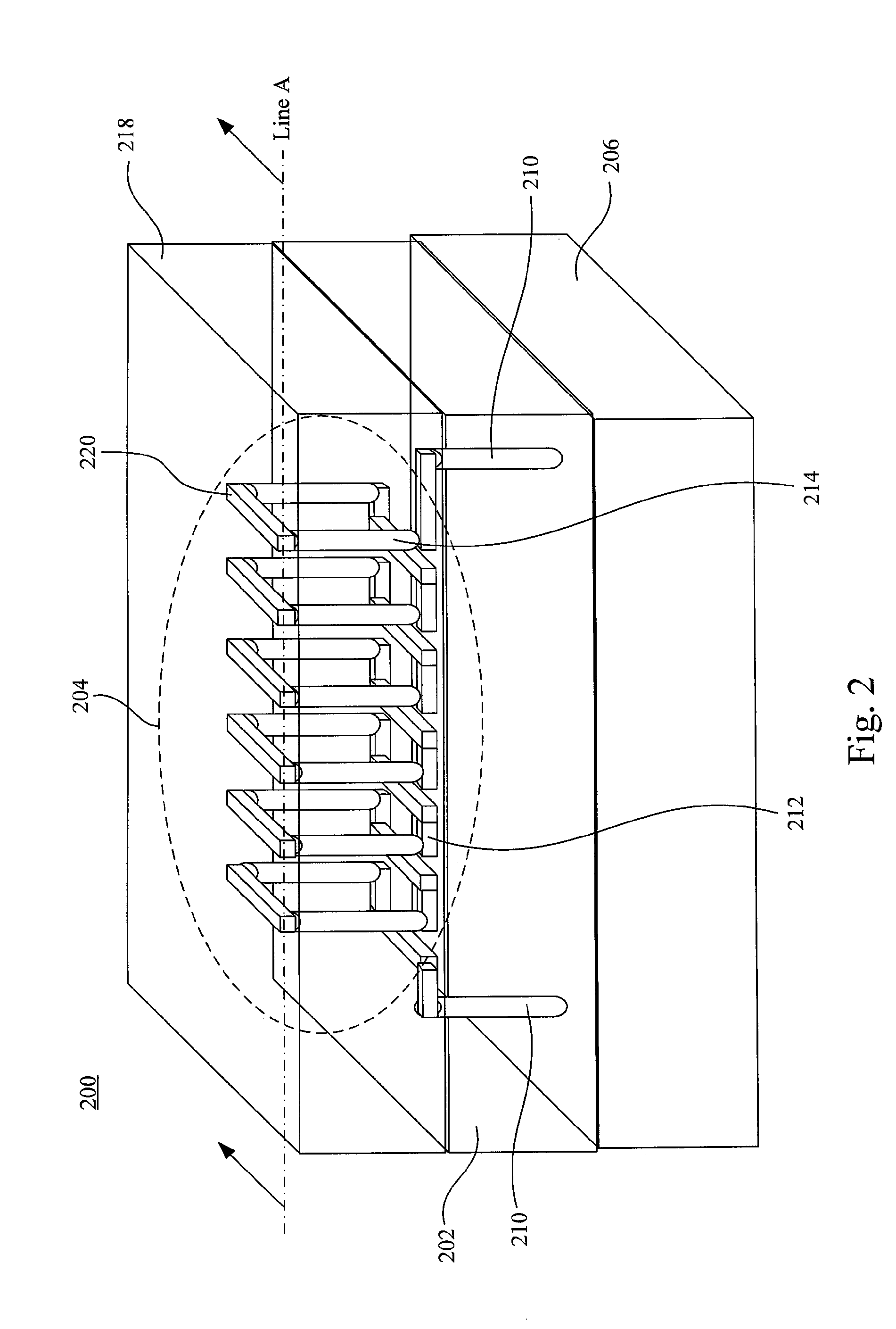
[0024]Please refer to FIG. 2, a 3-dimensional view of a conductive coil inductor manufactured by the method of the present invention. In this embodiment, the conductive coil inductor 200 may be of having a solenoid structure 204 elevated by a first dielectric layer 202 to distance the conductive coil structure 204 from the silicon substrate 206. In FIG. 2A, a cross section view along line A of the conductive coil inductor after the first step of manufacturing is shown. In the first step, a silicon substrate 206 is provided with two terminal contacts 208 thereon. The two terminal contacts 208 may be metal contacts electrically connected to applicable circuitry. Formed on the two terminal contacts 208 are two conductive connectors 210 to electrically connect the terminal contact 208 to the conductive coil structure 204. The two conductive connectors 210 may be formed by a lithography and metal plating process, such as copper plating. A first dielectric layer 202 is formed on the subst...

second embodiment

[0030]Therefore, if L is increased by inserting a ferromagnetic core with a large permeability, then Q will be increased accordingly. Thus the present invention shows an example of the method of manufacturing of a coil inductor with a ferromagnetic core 302.

[0031]Please refer to FIG. 3A, a cross-section view of along line B of the coil inductor 200 after the fifth step of manufacturing in the first embodiment of the present invention. The second dielectric layer 218 may be etched to form a trench 304 so to plant the ferromagnetic core 302 therein. This trench is optional and may be omitted and plant the ferromagnetic core 302 directly on the top surface of the second dielectric layer 218.

[0032]Please refer to FIG. 3B, a cross section view along line B of the coil inductor 200 in the first embodiment of the present invention. A photo-resist layer 306 is applied to the surface of the second dielectric layer 218. The photo-resist layer 306 is then etched above the trench 304 so to expo...


PUM

PropertyMeasurementUnit
thicknessaaaaaaaaaa
conductiveaaaaaaaaaa
dielectricaaaaaaaaaa

Abstract

A method of manufacturing a coil inductor and a coil inductor are provided are provided. A plurality of conductive bottom structures are formed to be lying on a first dielectric layer. A plurality pairs of conductive side structures are then formed, wherein each pair of the conductive side structure stand on top surface of a first end and a second end of each conductive bottom structure respectively; a second dielectric layer is formed on the first dielectric layer, coating the bottom and side structures; and a plurality of conductive top structures are formed to be lying on the second dielectric layer, wherein each conductive top structure electrically connects each pair of the conductive side structures, wherein the conductive bottom structures, the conductive side structures and the conductive top structures together form a conductive coil structure.

Description

BACKGROUND[0001]1. Field of Invention[0002]The present invention relates to a coil inductor. More particularly, the present invention relates to a method of manufacturing a coil inductor to reduce energy loss in the substrate.[0003]2. Description of Related Art[0004]Traditional inductors fabricated on silicon substrate are provided by coils of conductive material formed on the substrate. The coil of conductive material may be formed in a spiral structure as a spiral inductor in dielectric film. As illustrated in FIG. 1, a top view of a spiral inductor, the traditional spiral inductor is a spiral structure with the inductor coil 102 flatly laid out on the substrate surface 104. The two ends 106, 108 of the coil 102 may be electrically connected to conductive pads, respectively. The current flows through the inductor coil 102 introducing an inductance L and a quality factor Q. The current through the inductor coil also induces a small current known as the Eddy current flowing in the s...

Claims


Application Information

Patent Timeline
Patent Type & Authority Applications(United States)
IPC IPC(8): H01F41/04H01F41/02H01F41/00
CPCH01F17/0013Y10T29/4902H01F41/046H01F17/0033H01F2017/0086
Inventor CHING, KAI-MINGCHEN, CHEN-SHIEN
Owner TAIWAN SEMICON MFG CO LTD
Why Eureka
Try Eureka