Semiconductor device having insulated gate semiconductor element, and insulated gate bipolar transistor

Active Publication Date: 2009-07-30
DENSO CORP +1
View PDF17 Cites 43 Cited by
  • Summary
  • Abstract
  • Description
  • Claims
  • Application Information

AI Technical Summary

Benefits of technology

[0025]In the above transistor, the on-state voltage is low, which is almost equal to that of an IEGT. Furt

Problems solved by technology

However, when the dV/dt and dIc/dt are reduced, the switching loss increases.
Thus, it is difficult to reduce both of the electro magnetic noise and the switching loss.
Thus, the switching loss increases.
Thus, it is difficult to improve both of the on-state voltage and the switching characteristics.
Further, in general, the waveform of the device having the high-speed switching characteristics is hard when the device switches so that the device has a hard switching characteristics.
An electro magnet

Method used


Image

  • Semiconductor device having insulated gate semiconductor element, and insulated gate bipolar transistor
  • Semiconductor device having insulated gate semiconductor element, and insulated gate bipolar transistor
  • Semiconductor device having insulated gate semiconductor element, and insulated gate bipolar transistor

Examples


first embodiment

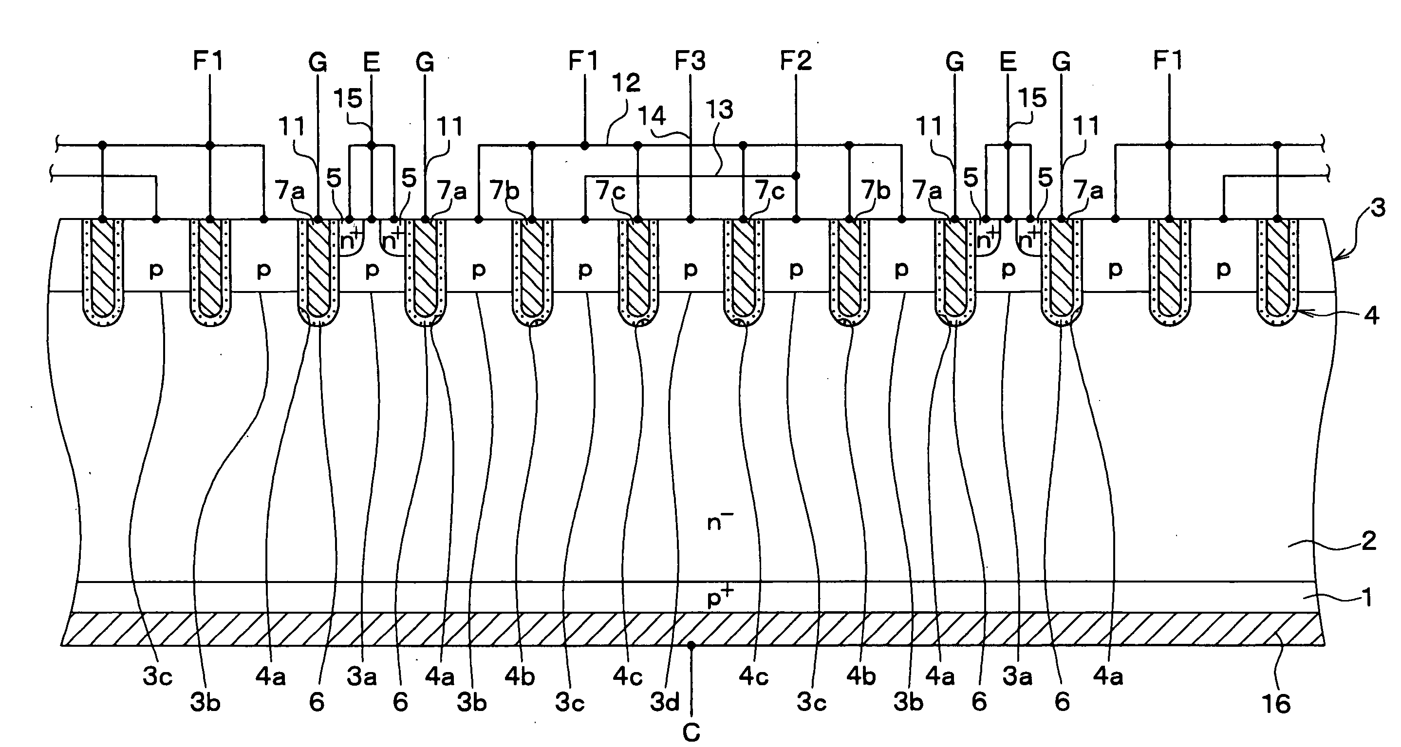
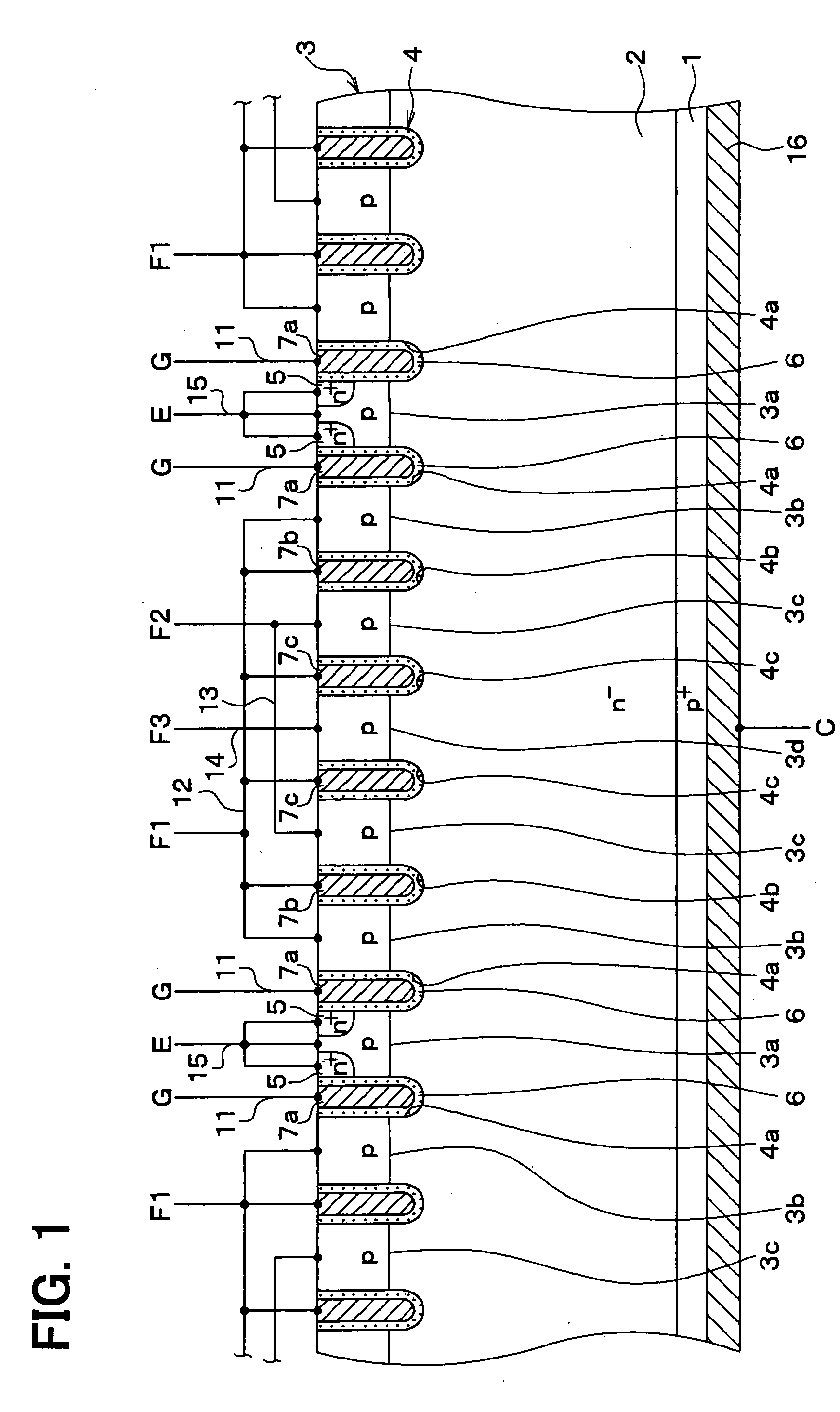
[0064]FIG. 1 shows a semiconductor device having an IGBT taken along line I-I in FIG. 3. FIG. 2 shows the device taken along line II-II in FIG. 3. Although FIG. 3 is not a cross sectional view, there is a hatching area in FIG. 3 to understand a structure easily.

[0065]An IGBT is formed in a P+ type substrate 1 having a principal surface. The substrate 1 has a high impurity concentration. A N− type drift layer 2 is formed on the principal surface of the substrate 1 by an epitaxial growth method. The drift layer 2 has a low impurity concentration, which is lower than the substrate 1.

[0066]A P type base region 3 having a predetermined thickness is formed in a surface portion of the drift layer 2. Multiple trenches 4 are formed on the substrate 1 such that each trench 4 penetrates the base region 3 and reaches the drift layer 2. The base region 3 is divided into multiple base portions by the trenches 4. Specifically, the trenches are arranged at predetermined intervals. Each trench 4 ext...

second embodiment

[0081]In a second embodiment, the gate electrode 7a, the dummy gate electrodes 7b, 7c and the first to third float layers 3b-3d are differently connected to each other, compared with the device in FIGS. 1-4.

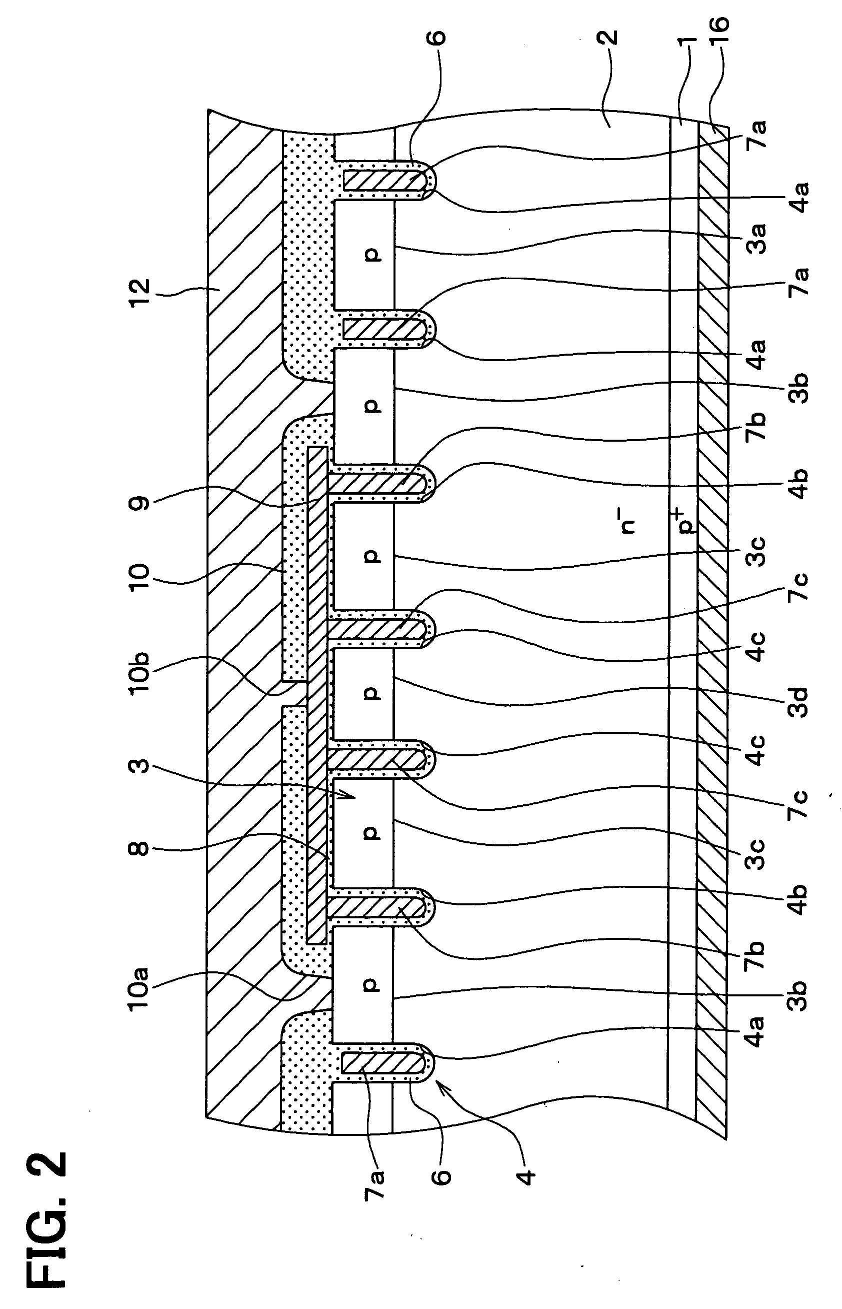
[0082]FIG. 5 shows a semiconductor device according to the second embodiment. FIG. 6 is a cross sectional view of the device taken along line VI-VI in FIG. 11, FIG. 7 is a cross sectional view of the device taken along line VII-VII in FIG. 11, FIG. 8 is a cross sectional view of the device taken along line VIII-VIII in FIG. 11, FIG. 9 is a cross sectional view of the device taken along line IX-IX in FIG. 11, and FIG. 10 is a cross sectional view of the device taken along line X-X in FIG. 11. FIG. 11 is not a cross sectional view, but a hatching is drawn in FIG. 11 to easily understand the drawing.

[0083]As shown in FIG. 5, the dummy gate electrode 7b formed in the first inner trench 4b is electrically connected to the first float layer 3b and the first float wiring 12. Further, th...

third embodiment

[0087]In a semiconductor device according to a third embodiment, the arrangement of the gate wiring 11, the first to third float wirings 12-14 and the emitter electrode 15 is different from that according to the first and second embodiments.

[0088]FIG. 12 shows the semiconductor device having an IGBT according to this embodiment. FIG. 12 is not a cross sectional view, but, in FIG. 12, the view is partially hatched to easily understand the drawing. The first to third float wirings are disposed on both sides of the emitter electrode 15 so that they sandwich the emitter electrode 15. Further, the gate wiring 11 is disposed on both sides of the emitter electrode 15 and the first to third float wirings 12-14 so that the gate wiring 11 sandwiches the emitter electrode 15 and the first to third float wirings 12-14. The device further includes a gate pad 11a for connecting the gate wiring 11 and an external circuit, a first float pad 12a for connecting the first float wiring 12 and the exter...


PUM


Abstract

A semiconductor device having an IGBT includes: a substrate; a drift layer and a base layer on the substrate; trenches penetrating the base layer to divide the base layer into base parts; an emitter region in one base part; a gate element in the trenches; an emitter electrode; and a collector electrode. The one base part provides a channel layer, and another base part provides a float layer having no emitter region. The gate element includes a gate electrode next to the channel layer and a dummy gate electrode next to the float layer. The float layer includes a first float layer adjacent to the channel layer and a second float layer apart from the channel layer. The dummy gate electrode and the first float layer are coupled with a first float wiring on the base layer. The dummy gate electrode is isolated from the second float layer.

Description

CROSS REFERENCE TO RELATED APPLICATIONS[0001]This application is based on Japanese Patent Applications No. 2008-015760 filed on Jan. 28, 2008, No. 2008-271135 filed on Oct. 21, 2008, and No. 2008-287036 filed on Nov. 7, 2008, the disclosures of which are incorporated herein by reference.FIELD OF THE INVENTION[0002]The present invention relates to a semiconductor device having an insulated gate semiconductor element, and an insulated gate bipolar transistor.BACKGROUND OF THE INVENTION[0003]An insulated gate semiconductor device such as a trench gate type transistor and an IGBT functions as a high break down voltage insulated gate semiconductor device having a trench gate structure. FIGS. 17 and 18 show IGBTs disclosed in JP-A-2006-49455. Each IGBT includes an N+ type emitter region 101 for contacting an emitter electrode is selectively formed in a P type base region 102. A dummy trench 103 is formed in a region other than the emitter region 101. Thus, multiple trenches are homogeneou...

Claims


Application Information

Patent Timeline
IPC IPC(8): H01L29/739
CPCH01L29/0696H01L29/7395H01L29/66348H01L29/0619H01L29/402H01L29/407H01L29/4238H01L29/7397
Inventor KOYAMA, MASAKIOKABE, YOSHIFUMIASAI, MAKOTOFUJII, TAKESHIYOSHIKAWA, KOH
Owner DENSO CORP
Why Eureka
Try Eureka