

Piezoelectric Thin Film Device
a thin film, piezoelectric technology, applied in the direction of turn-sensitive devices, instruments, devices, etc., can solve the problems of accelerating device degradation, affecting the performance of high-sensitivity sensors, and fluctuation in piezoelectric properties, so as to increase the piezoelectric constant d31, suppress the dependence of piezoelectric constant d31, and high performance
- Summary
- Abstract
- Description
- Claims
- Application Information
AI Technical Summary
Benefits of technology
Problems solved by technology
Method used
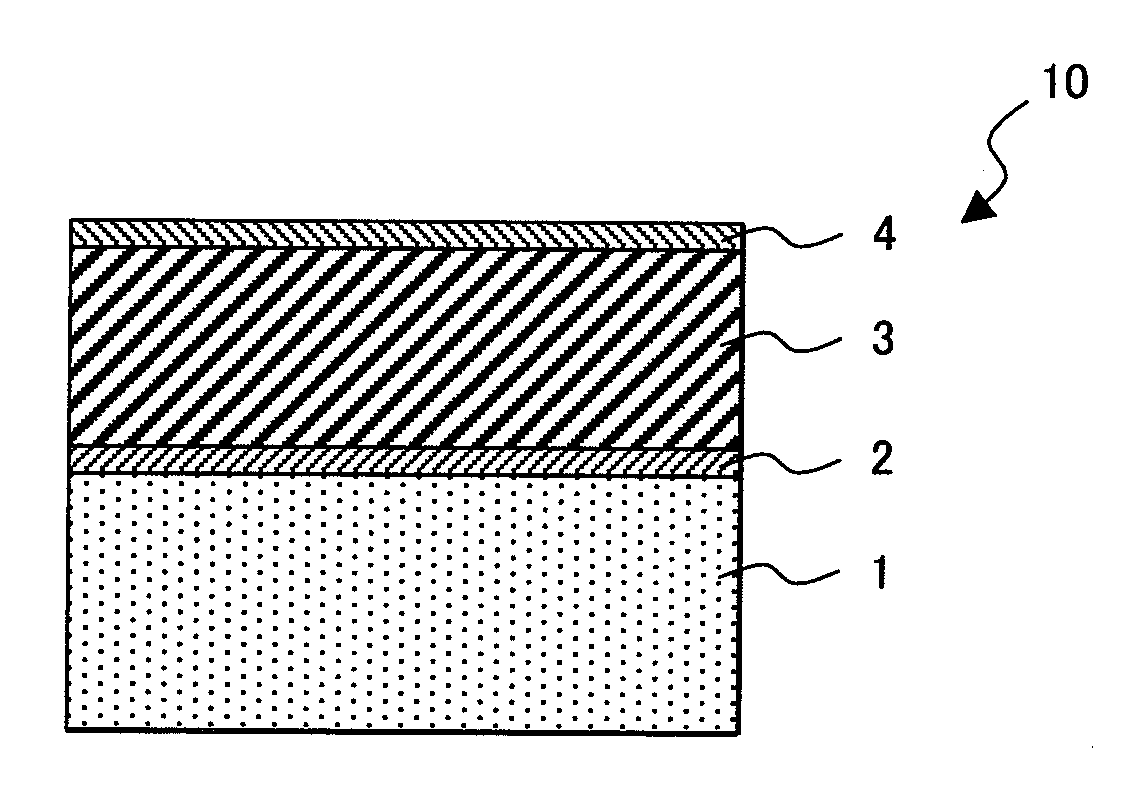
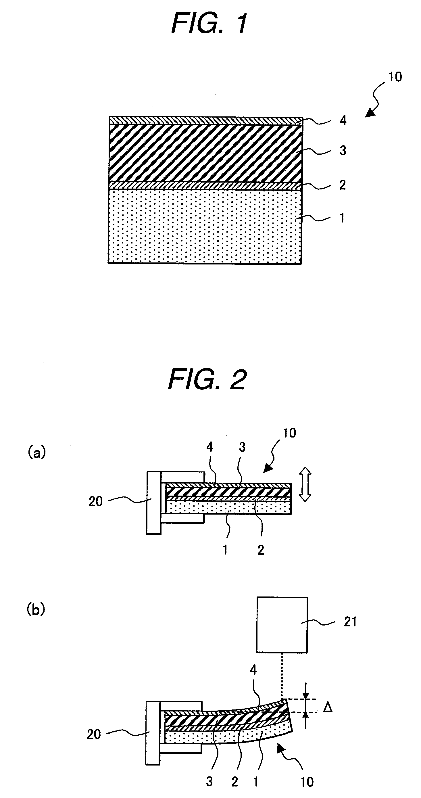
Image

Examples
examples
[0053]Examples of the invention will be described below, however the present invention is not limited by these examples.
Examples and Comparative Examples of Piezoelectric Thin Film Device Having Structure in FIG. 3
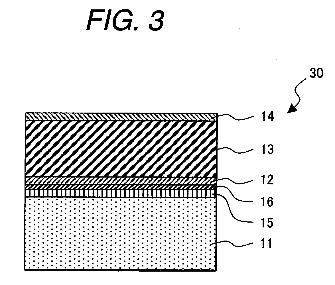
[0054]FIG. 3 is a schematic illustration showing a cross-sectional view of the piezoelectric thin film device of Examples 1 to 4 and Comparative examples 1 to 6. The piezoelectric thin film devices 30 of Examples 1 to 4 and Comparative examples 1 to 6 were fabricated by sequentially forming, on an Si substrate 11 (having an SiO2 film 15 on its surface), a Ti adhesive layer 16, a Pt lower electrode 12, a (K0.5Na0.5)NbO3 piezoelectric thin film 13, and a Pt upper electrode 14.
[0055]Next, the fabrication method of the piezoelectric thin film device of Examples 1 to 4 will be detailed.
[0056]As the Si substrate 11, there was used an Si substrate with a thermal oxide layer (an SiO2 film 15) on the substrate surface ((100)Si single crystalline substrate of 4-inch round wafer, sub...
PUM
 Abstract
Description
Claims
Application Information