
Organic light emitting diode and method of manufacturing the same

a light-emitting diode and organic technology, applied in the direction of discharge tube/lamp details, discharge tube luminescnet screens, organic chemistry, etc., can solve the problems of poor luminous efficiency, insufficient lifespan, difficult to achieve high-quality oleds, etc., to increase luminous efficiency and lifespan, reduce driving voltage and current consumption

Active Publication Date: 2009-07-30
SAMSUNG DISPLAY CO LTD
View PDF27 Cites 9 Cited by
  • Summary
  • Abstract
  • Description
  • Claims
  • Application Information

AI Technical Summary

Benefits of technology

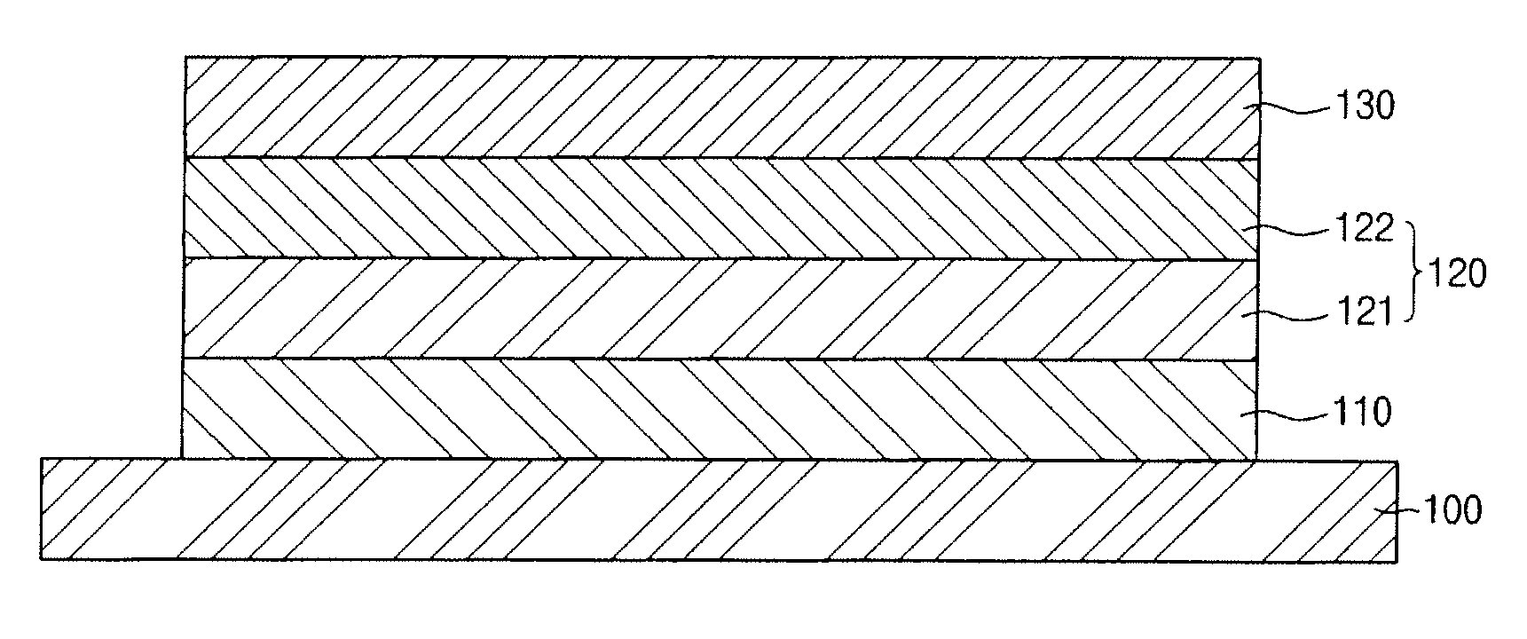
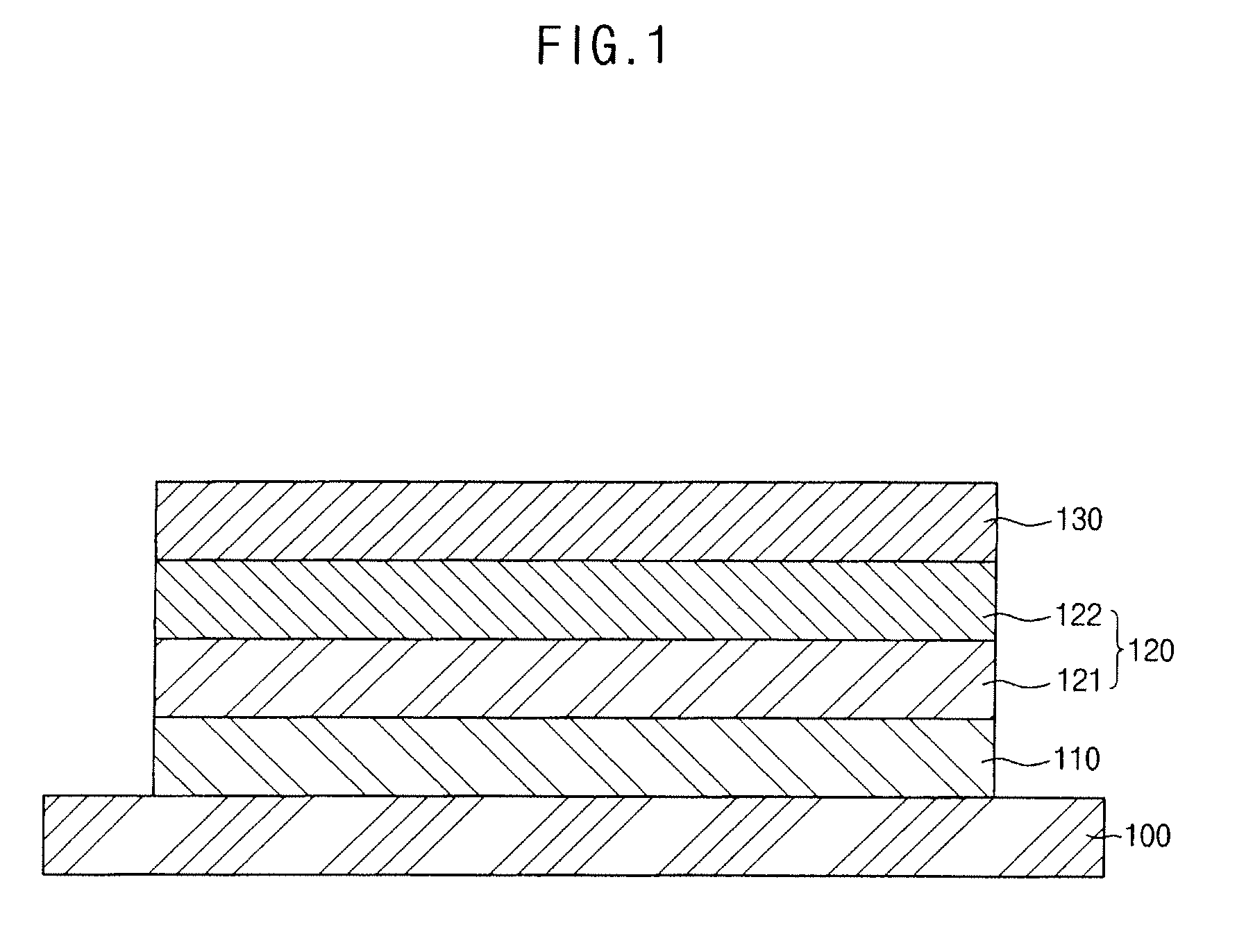
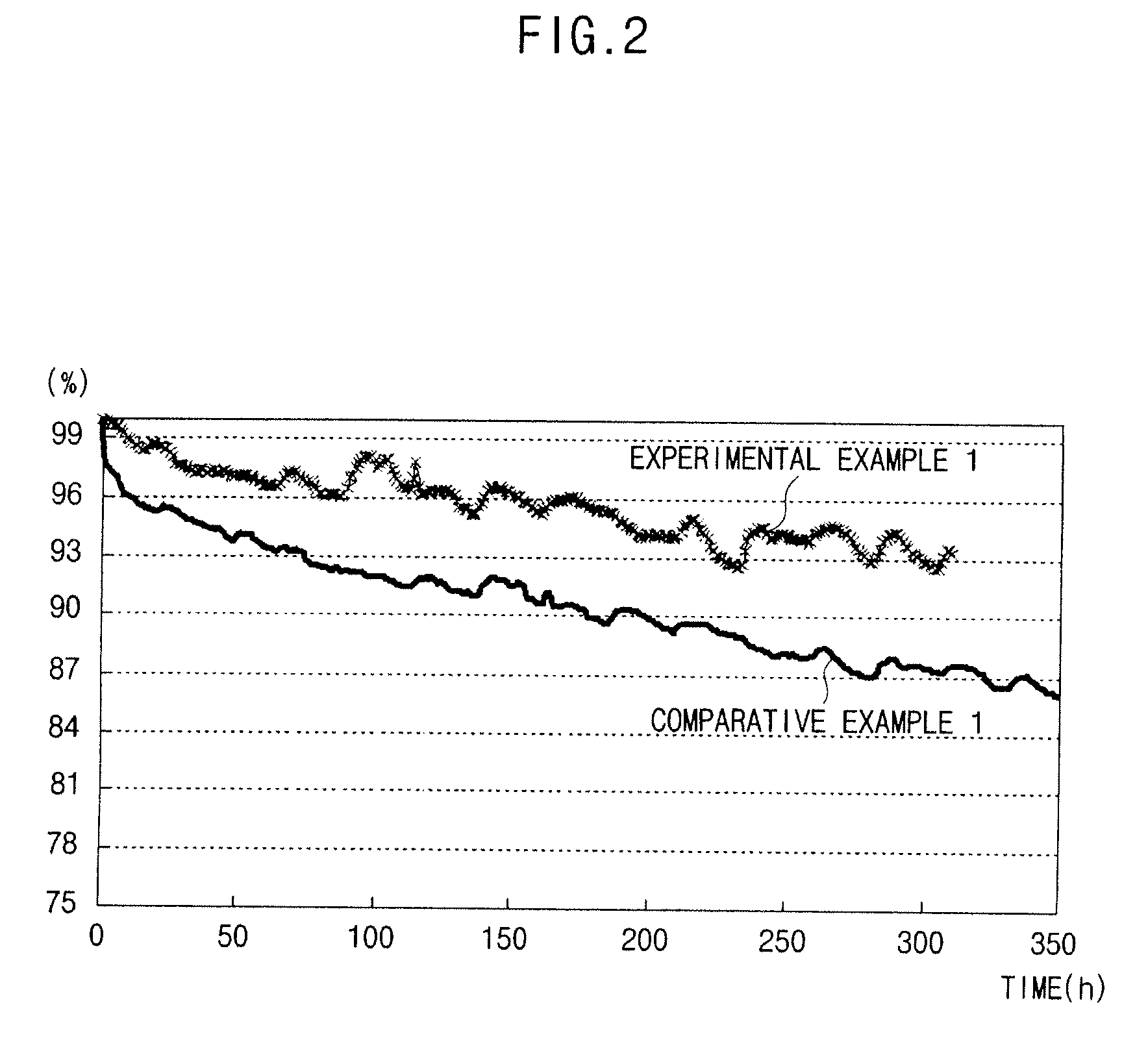
[0009]Embodiments of the present invention provide an organic light emitting diode (OLED) and a method of manufacturing the same. In one embodiment, an improved electron transport layer (ETL) reduces driving voltage and current consumption, thereby increasing the luminous efficiency and lifespan of the OLED.

Problems solved by technology

As a result, the OLED including the ETL needs to drive at a high driving voltage and consume a large current, imparting poor luminous efficiency and insufficient lifespan.
Therefore, high quality OLEDs are difficult to achieve.

Method used


Image

  • Organic light emitting diode and method of manufacturing the same
  • Organic light emitting diode and method of manufacturing the same
  • Organic light emitting diode and method of manufacturing the same

Examples


experimental example 1

[0039]A first electrode was formed of ITO to a thickness of about 130 nm. Thereafter, an HIL was formed of IDE-406 (obtained from Idemitsu Co.) on the first electrode to a thickness of about 210 nm, and an HTL was formed of NPB to a thickness of about 20 nm. A red EML was formed on the HTL to a thickness of about 40 nm using a mixture of CBP as a host and 15% by weight Ir(piq)3 as a dopant. An ETL was formed on the red EML. Specifically, 50% by weight of lithium quinolate as an organic metal complex containing an alkali metal, and 50% by weight of a compound of Formula 1 were co-deposited to a thickness of about 30 nm. In the compound of Formula 1, R9 is a phenyl group to which a benzimidazolyl group is bonded, and each of R1 to R8 and R10 to R22 is hydrogen. Subsequently, a second electrode was formed on the ETL. To form the second electrode, an MgAg layer was formed to a thickness of about 16 nm, and an Al layer was formed on the MgAg layer to a thickness of about 100 nm.

experimental example 2

[0044]A first electrode was formed of ITO to a thickness of about 130 nm. Thereafter, an HIL was formed of IDE-406 (obtained from Idemitsu Co.) on the first electrode to a thickness of about 210 nm, and an HTL was formed of NPB to a thickness of about 20 nm. A red EML was formed on the HTL to a thickness of about 30 nm using a mixture of CBP as a host and 8% by weight lr(piq)3 as a dopant. An ETL was formed on the red EML. Specifically, 25% by weight of sodium quinolate (which is an organic metal complex containing an alkali metal) and 75% by weight of a compound of Formula 1 were co-deposited to a thickness of about 30 nm. In the compound of Formula 1, R9 is a phenyl group to which a benzimidazolyl group is bonded, and each of R1 to R8 and R10 to R22 is hydrogen.

[0045]Subsequently, a second electrode was formed on the ETL. To form the second electrode, an MgAg layer was formed to a thickness of about 16 nm, and an Al layer was formed on the MgAg layer to a thickness of about 100 nm...

experimental example 3

[0049]A first electrode was formed of ITO to a thickness of about 130 nm. Thereafter, an HIL was formed of IDE-406 (obtained from Idemitsu Co.) on the first electrode to a thickness of about 210 nm, and an HTL was formed of NPB to a thickness of about 20 nm. A red EML was formed on the HTL to a thickness of about 30 nm using a mixture of CBP as a host and 8% by weight lr(piq)3 as a dopant. An ETL was formed on the red EML. Specifically, 50% by weight of sodium quinolate (which is an organic metal complex containing an alkali metal) and 50% by weight of a compound of Formula 1 were co-deposited to a thickness of about 30 nm. In the compound of Formula 1, R9 is a phenyl group to which a benzimidazolyl group is bonded, and each of R1 to R8 and R10 to R22 is hydrogen.

[0050]Subsequently, a second electrode was formed on the ETL. To form the second electrode, an MgAg layer was formed to a thickness of about 16 nm, and an Al layer was formed on the MgAg layer to a thickness of about 100 nm...


PUM

PropertyMeasurementUnit
thicknessaaaaaaaaaa
thicknessaaaaaaaaaa
thicknessaaaaaaaaaa

Abstract

The invention is directed to organic light emitting diodes (OLEDs) and methods of manufacturing the same. According to embodiments of the invention, an improved electron transport layer (ETL) reduces the driving voltage and current consumption of the OLED, and increase luminous efficiency and lifespan. The OLED includes a first electrode, an organic layer on the first electrode and including an emission layer (EML) and an ETL, and a second electrode on the organic layer.

Description

CROSS-REFERENCE TO RELATED APPLICATION[0001]This application claims priority to and the benefit of Korean Patent Application No. 2008-0008722, filed Jan. 28, 2008 in the Korean Intellectual Property Office, the entire content of which is incorporated herein by reference.BACKGROUND OF THE INVENTION[0002]1. Field of the Invention[0003]The present invention relates to organic light emitting diodes (OLEDs) and methods of manufacturing the same.[0004]2. Description of the Related Art[0005]Organic light emitting diodes (OLEDs) are self-emissive displays that may be lightweight and thin, and fabricated by simple processes using simple components. Also, OLEDs have high resolution and wide viewing angles, and can embody complete moving images with high color purity. In addition, OLEDs have appropriate electrical characteristics for mobile display devices because OLEDs consume little power and drive at low voltages.[0006]In a conventional OLED, a pixel electrode is provided, an organic layer ...

Claims


Application Information

Patent Timeline
Patent Type & Authority Applications(United States)
IPC IPC(8): H01J1/63B05D5/06
CPCC07C15/28H01L51/5052H01L51/0058H10K85/626H10K50/165C09K11/06C07C13/54C09K2211/1011C09K2211/1025C09K2211/1081H10K85/30H10K50/16H10K50/11H10K50/00
Inventor CHUN, MIN-SEUNGKIM, DONG-HEONKWAK, JAE-HYUNSON, JUNG-HAKIM, MI-KYUNGLEE, KWAN-HEE
Owner SAMSUNG DISPLAY CO LTD
Learn More