Semiconductor integrated circuit device having standard cell including resistance element

a technology of integrated circuit and resistance element, which is applied in the direction of pulse manipulation, pulse technique, instruments, etc., can solve the problems of increasing the number of errors that might occur at the receiving side, unbalanced digital signal waveform duty ratio, and increasing the difficulty of keeping setup time and hold time. , to achieve the effect of reducing the number of designing processes

Inactive Publication Date: 2009-08-06
RENESAS ELECTRONICS CORP
View PDF2 Cites 12 Cited by
  • Summary
  • Abstract
  • Description
  • Claims
  • Application Information

AI Technical Summary

Benefits of technology

[0011]According to the exemplary aspect of the present invention, because the semiconductor integrated circuit device is configured so that a transistor resistance area is laid out beforehand and transistor resist

Problems solved by technology

In case of such a DDR system, however, when the signal waveform duty ratio is deviated from 50%, it is becoming difficult more and more to keep the setup time and hold time, for example, in the input side flip-flop process or the like.
In case of a system used for fast clock transmissions, if the signal waveform duty ratio is deviated from 50%, then the eye aperture rate falls, thereby the number of errors that might occur at the receiving side comes to increase.
In such a semiconductor integrated circuit device, the signal waveform duty ratio c

Method used


Image

  • Semiconductor integrated circuit device having standard cell including resistance element
  • Semiconductor integrated circuit device having standard cell including resistance element
  • Semiconductor integrated circuit device having standard cell including resistance element

Examples


first exemplary embodiment

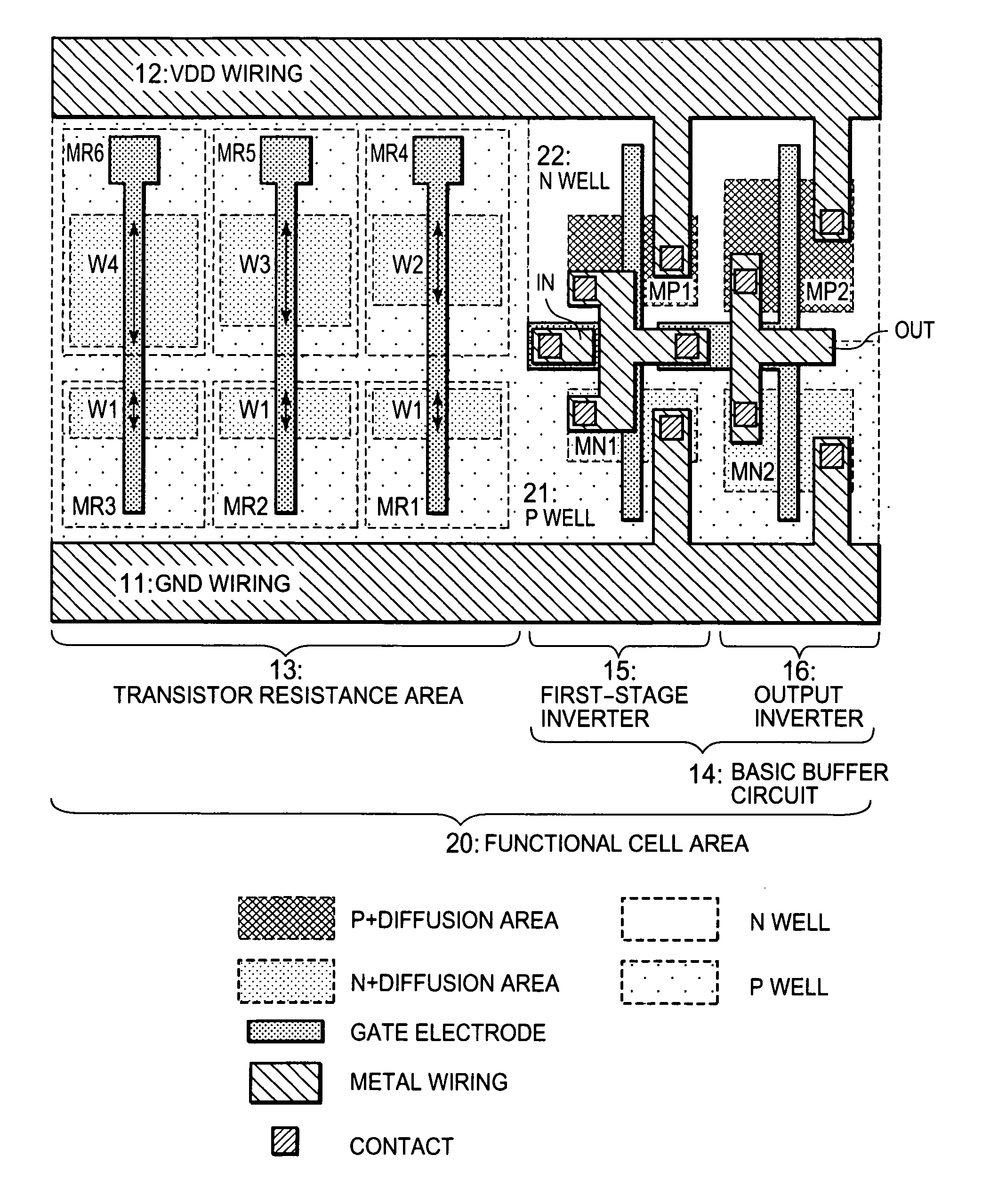
[0045]FIG. 1 shows a basic layout of a semiconductor integrated circuit device in this first exemplary embodiment of the present invention. In FIG. 1, the semiconductor integrated circuit device includes a rectangular functional cell area 20 between a GND wiring 11 and a VDD wiring 12 laid in parallel to the GND wiring 11. The functional cell area 20 includes a transistor resistance area 13 and a basic buffer circuit 14 that are adjacent to each other.

[0046]The transistor resistance area 13 includes an approximately rectangular P well 21 having two sides that are part of the GND wiring 11 and part of the VDD wiring 12, as well as a plurality of NMOS transistor resistances MR1 to MR6 provided in the P well 21. In FIG. 1, the NMOS transistor resistances MR1 to MR6 mean transistors made of transistors respectively in an N+diffusion area in a transistor disposition area. Here, the gate of a transistor in the transistor resistance area 13 has a fixed length L and an interval. The N+ diff...

second exemplary embodiment

[0077]FIG. 16 shows a basic layout of a semiconductor integrated circuit device in this second exemplary embodiment of the present invention. In FIG. 16, the same reference numerals will be used for the same components as those shown in FIG. 1, avoiding redundant description. In FIG. 16, the semiconductor integrated circuit device includes a rectangular functional cell area 20a provided between a GND wiring 11 and a VDD wiring 12 laid in parallel to the GND wiring 11. The functional cell area 20a includes a transistor resistance area 13a and a basic buffer circuit 14 that are adjacent to each other.

[0078]The transistor resistance area 13a includes approximately rectangular N well having two sides that are part of the GND wiring 11 and part of the VDD wiring 12, as well as PMOS transistor resistances MR11 to MR16 provided in this N well. In FIG. 16, a region equivalent to the N well 22 shown in FIG. 1 and the N well in the transistor resistance area 13a are integrated into one (as an...


PUM


Abstract

A standard cell includes an input terminal, an output terminal, first and second inverters coupled in series between the input and output terminals, the first inverter including a first transistor of a first conductivity type and a second transistor of a second conductivity type, the first transistor being coupled between a first power source terminal and a first node, and the second transistor being coupled between a second node and a second power source terminal, and a plurality of resistance elements which are used to provide a conductivity path between the first and second nodes, in order to adjust a duty ratio of a signal which passes the standard cell.

Description

BACKGROUND OF THE INVENTION[0001]1. Field of the Invention[0002]The present invention relates to a semiconductor integrated circuit device, more particularly to a semiconductor integrated circuit device having a circuit used for delay adjustments.[0003]2. Description of Related Art[0004]When designing a DDR (Double Data Rate) system or the like, both rising and falling edges of signals are used. In case of such a DDR system, however, when the signal waveform duty ratio is deviated from 50%, it is becoming difficult more and more to keep the setup time and hold time, for example, in the input side flip-flop process or the like. In case of a system used for fast clock transmissions, if the signal waveform duty ratio is deviated from 50%, then the eye aperture rate falls, thereby the number of errors that might occur at the receiving side comes to increase. Consequently, such a system is usually required to have a function for adjusting the output signal duty ratio so as to be fixed at...

Claims


Application Information

Patent Timeline
IPC IPC(8): H03K5/04H03H11/00
CPCH01L27/11898H01L27/0207
Inventor TATSUMI, KYOKA
Owner RENESAS ELECTRONICS CORP
Why Eureka
Try Eureka