Method of fabricating a semiconductor device

a technology of semiconductor devices and gate components, which is applied in the direction of semiconductor devices, electrical appliances, nanotechnology, etc., can solve the problems of affecting the performance/quality of semiconductor devices, and achieve the effect of facilitating the formation of inner and outer junction regions

Inactive Publication Date: 2009-08-06
SAMSUNG ELECTRONICS CO LTD
View PDF5 Cites 17 Cited by
  • Summary
  • Abstract
  • Description
  • Claims
  • Application Information

AI Technical Summary

Benefits of technology

[0010]According to another aspect of the present invention, there is provided a method of fabricating a semiconductor device which includes forming a pair of gates on a substrate, and forming asymmetric junction regions in the substrate on opposite sides of each gate. The asymmetric junction regions include an inner junction region located between the pair of gates, and outer junction regions laterally outwardly of the pair of gates. Each of the outer junction regions is asymmetric to the inner junction region with respect to a plane t...

Problems solved by technology

The performance/quality of a semiconductor dev...

Method used


Image

  • Method of fabricating a semiconductor device
  • Method of fabricating a semiconductor device
  • Method of fabricating a semiconductor device

Examples


Embodiment Construction

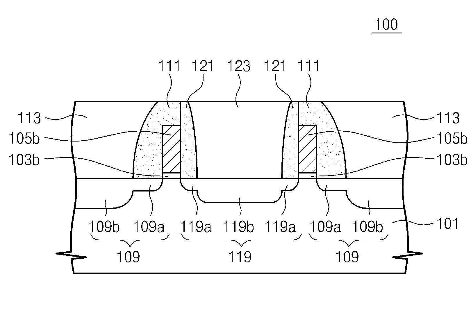
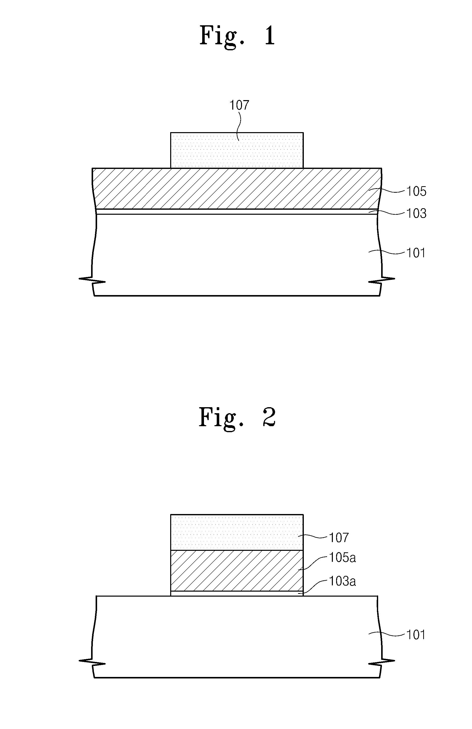
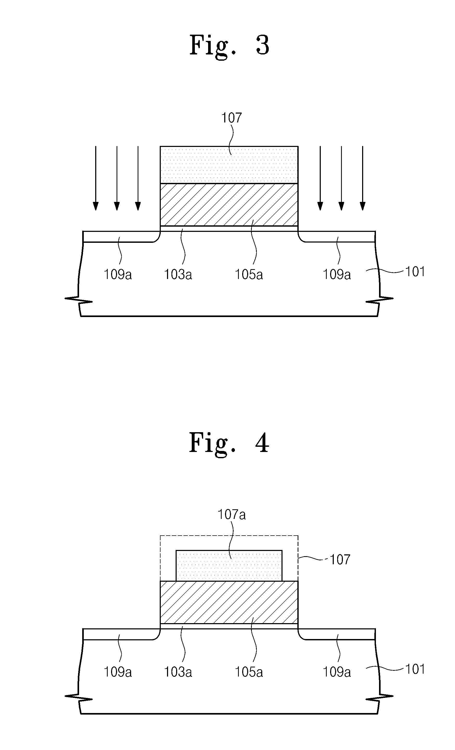
[0020]A method of forming a gate of a semiconductor device according to the present invention will now be described with reference to the figures. Referring first to FIG. 1, an oxide layer 103 is formed on a substrate 101. For example, the substrate 101 is a semiconductor substrate such as a silicon wafer, and the oxide layer 103 is a silicon oxide layer. Also, an active region is defined in the substrate 101 by a device isolation layer (not shown).

[0021]Next, a conductive layer 105 is formed on the oxide layer 103, and a gate mask 107 is formed on the conductive layer 105. The conductive layer 105 may be formed by depositing polysilicon on the oxide layer 103, and the gate mask 107 may be formed by depositing silicon nitride on the conductive layer and patterning the resulting layer of silicon nitride.

[0022]Referring to FIG. 2, the conductive layer 105 and the oxide layer 103 may be simultaneously etched, by a dry etch process that employs the gate mask 107 as an etch mask, to form...


PUM


Abstract

A method of fabricating a semiconductor device forms a micro-sized gate, and mitigates short channel effects. The method includes a pull-back process to form the gate on a substrate. The method also includes forming inner and outer spacers on the gate that are asymmetric to one another with respect to the gate, and using the spacers in forming junction regions in the substrate on opposite sides of the gate. In particular, the inner and outer spacers are formed on opposite sides of the gate so as to have different thicknesses at the bottom of the gate. The inner and outer junction regions are formed by doping the substrate before and after the spacers are formed. Thus, the inner and outer junction regions have extension regions under the inner and outer spacers, respectively, and the extension regions have different lengths.

Description

BACKGROUND OF THE INVENTION[0001]1. Field of the Invention[0002]The present invention relates to a method of fabricating a semiconductor device. More particularly, the present invention relates to a method of fabricating a micro-sized gate of a transistor.[0003]2. Description of the Related Art[0004]The gates of transistors of semiconductor devices are gradually becoming smaller as semiconductor devices in general become more highly integrated. As a result, the significance of the affect of the electric field of a junction region on electric potential in a channel region of a transistor may increase. For example, the scaling down of a transistor may give rise to short channel effects such as the lowering of the threshold voltage of the transistor and / or punch through. The performance / quality of a semiconductor device may be undermined by such short channel effects.SUMMARY OF THE INVENTION[0005]An object of the present invention is to provide a method of fabricating a micro-sized gat...

Claims


Application Information

Patent Timeline
IPC IPC(8): H01L21/336H01L21/335
CPCH01L21/28123H01L21/823425H01L21/823437H01L29/7835H01L29/42376H01L29/66659H01L21/823468B82Y40/00H01L21/18H01L21/265
Inventor KIM, SUNG-MINKIM, MIN-SANGCHO, KEUN-HWILEE, JI-MYOUNG
Owner SAMSUNG ELECTRONICS CO LTD
Why Eureka
Try Eureka