Method of manufacturing device

a manufacturing method and technology of a device, applied in the field of manufacturing a device, can solve the problems of affecting and the device thus cut apart may show irregular motions on the adhesive film, so as to achieve the effect of lowering the transverse rupture strength of the device and not lowering the quality of the devi

Active Publication Date: 2009-08-06
DISCO CORP
View PDF1 Cites 43 Cited by
  • Summary
  • Abstract
  • Description
  • Claims
  • Application Information

AI Technical Summary

Benefits of technology

[0009]Accordingly, it is an object of the present invention to provide a method of manufacturing a device by which devices each having an adhesive film attached to the back-side surface thereof can be manufactured without lowering device quality and without lowering the transverse rupture strength of the devices.

Problems solved by technology

However, when the adhesive film is adhered to the back-side surface of the wafer and the resulting assembly is cut by the cutting blade, the devices thus cut apart may show irregular motions on the adhesive film.
Particularly, in the case where the thickness of the wafer is as small as 100 μm or below, the devices may be broken by the shock of the cutting blade which is rotating at a high speed.
This approach, however, has the following problems.
When the wafer is irradiated with the pulsed laser beam having such a wavelength as to be absorbed in the wafer from the face side of the wafer along the planned dividing lines, thermal energy would be concentrated on the irradiated region with the result of generation of debris, and the debris would adhere to device surfaces, thereby lowering the device quality.

Method used


Image

  • Method of manufacturing device
  • Method of manufacturing device
  • Method of manufacturing device

Examples


Embodiment Construction

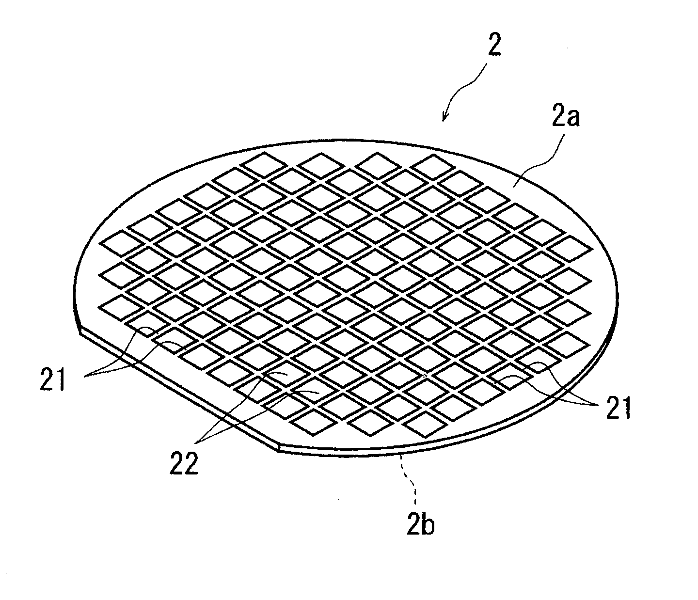
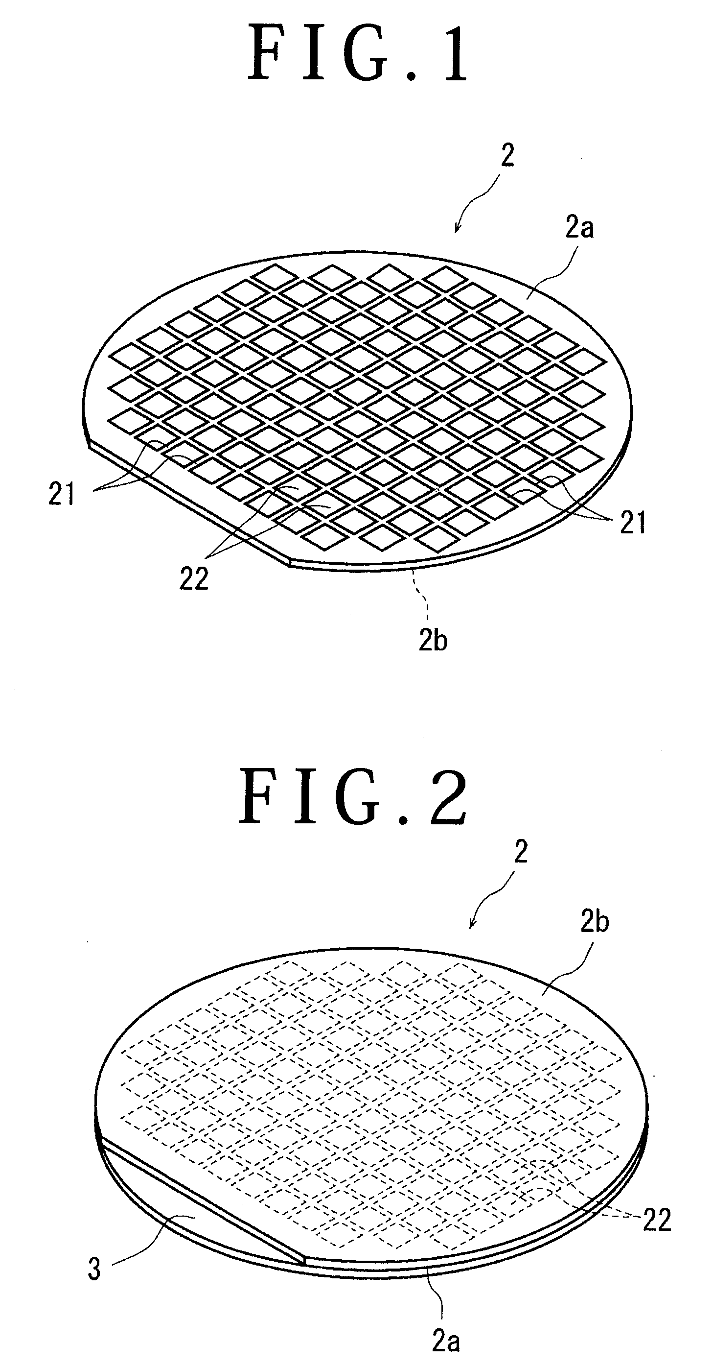
[0026]Now, preferred embodiments of the method of manufacturing a device according to the present invention will be described in detail below, referring to the attached drawings. FIG. 1 shows a perspective view of a semiconductor wafer as a wafer. The semiconductor wafer 2 shown in FIG. 1 is composed, for example, of a silicon wafer having a thickness of 80 μm, and its face-side surface 2a is provided with a plurality of planned dividing lines 21 in a grid pattern. At the face-side surface 2a of the semiconductor wafer 2, devices 22 such as ICs and LSIs are formed in the plurality of regions demarcated by the plurality of planned dividing lines 21 formed in the grid pattern. To the surface 2a of the semiconductor wafer 2 as above, a protective tape 3 is adhered as shown in FIG. 2 for the purpose of protecting the devices 22 (protective tape adhering step).

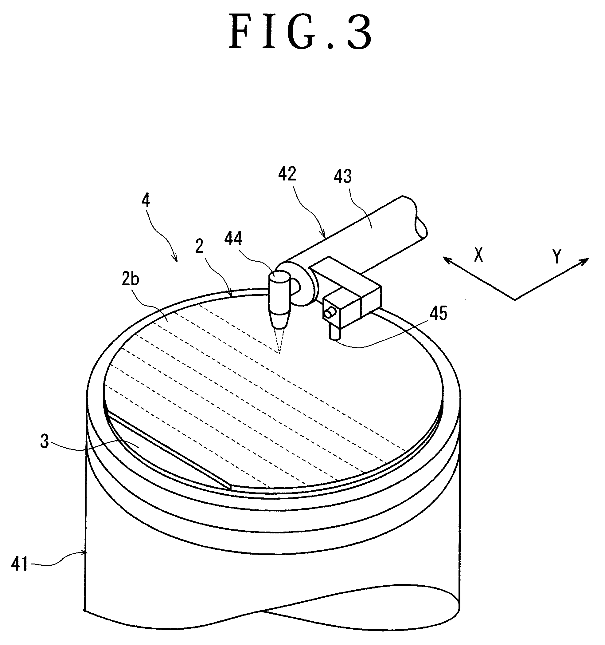
[0027]After the protective tape 3 is adhered to the face-side surface 2a of the semiconductor wafer 2 by conducting the protectiv...


PUM

PropertyMeasurementUnit
thicknessaaaaaaaaaa
thicknessaaaaaaaaaa
thicknessaaaaaaaaaa

Abstract

A method of manufacturing a device includes: a laser beam-machined groove forming step of irradiating a wafer with a laser beam from the back side of the wafer along planned dividing lines so as to form laser beam-machined grooves along the planned dividing lines; an etching step of etching a back-side surface of the wafer having been subjected to the laser beam-machined groove forming step, so as to remove denatured layers formed at processed surfaces of the laser beam-machined grooves; an adhesive film attaching step of attaching an adhesive film to the back-side surface of the wafer having been subjected to the etching step, and adhering the adhesive film side of the wafer to a surface of a dicing tape; and an adhesive film rupturing step of expanding the dicing tape so as to rupture the adhesive film along individual devices.

Description

BACKGROUND OF THE INVENTION[0001]1. Field of the Invention[0002]The present invention relates to a method of manufacturing a device by which a wafer having devices formed in a plurality of regions demarcated by planned dividing lines formed in a grid pattern on the face-side surface of the wafer is divided along the planned dividing lines into individual devices and an adhesive film for die bonding is attached to the back-side surface of each of the devices.[0003]2. Description of the Related Art[0004]In a semiconductor device manufacturing process, for example, it is a common practice to form devices such as ICs (integrated circuits) and LSIs (large-scale integrations) in a plurality of regions demarcated by streets (planned dividing lines) formed in a grid pattern on the face-side surface of a substantially circular disk-shaped semiconductor wafer, and to divide the regions with the devices formed therein along the planned dividing lines, thereby manufacturing the individual devic...

Claims


Application Information

Patent Timeline
Patent Type & Authority Applications(United States)
IPC IPC(8): H01L21/782B23K26/364B23K26/38
CPCB23K26/0853B23K26/367B23K26/4075H01L21/78H01L21/3065H01L21/67092H01L21/67132B23K2201/40B23K26/364B23K26/40B23K2101/40B23K2103/50
Inventor NAKAMURA, MASARUMATSUMOTO, HIROKAZU
Owner DISCO CORP
Why Eureka
Try Eureka