Semiconductor device and manufacturing method thereof

a technology of semiconductor devices and semiconductors, applied in semiconductor devices, semiconductor/solid-state device details, electrical apparatus, etc., can solve the problems of reducing gate capacitance, inferior performance, and conventional poly-silicon gate faces, and achieve the effect of enhancing process yield and device quality

Inactive Publication Date: 2013-03-14
UNITED MICROELECTRONICS CORP
View PDF4 Cites 37 Cited by
  • Summary
  • Abstract
  • Description
  • Claims
  • Application Information

AI Technical Summary

Benefits of technology

[0012]In the present invention, the metal gate structure may avoid being damaged during forming the contact holes because the replacement metal gate process is completed after forming the contact holes. The process window of the etching process for forming the contact hole may accordingly improved, and the process yield and the device quality may also be enhanced.

Problems solved by technology

With the trend towards scaling down the size of semiconductor devices, however, conventional poly-silicon gates face problems such as inferior performance due to boron penetration and unavoidable depletion effect.
This increases equivalent thickness of the gate dielectric layer, reduces gate capacitance, and worsens a driving force of the devices.
After performing the anneal process with a strict heat budget, it is found that a flat band voltage (Vfb) does not increase or decrease linearly with decreasing EOT of the high-k gate dielectric layer; instead, a roll-off issue is observed.
An inter-layer dielectric with a substantial thickness over the diffusion region has to be penetrated by the contact plug, and it becomes more difficult to control the etching process.

Method used


Image

  • Semiconductor device and manufacturing method thereof
  • Semiconductor device and manufacturing method thereof
  • Semiconductor device and manufacturing method thereof

Examples


Embodiment Construction

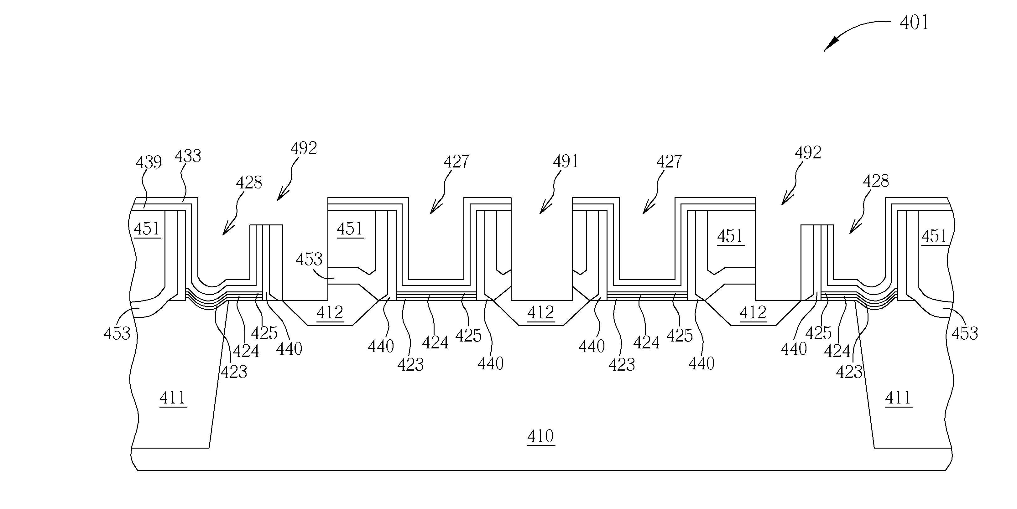
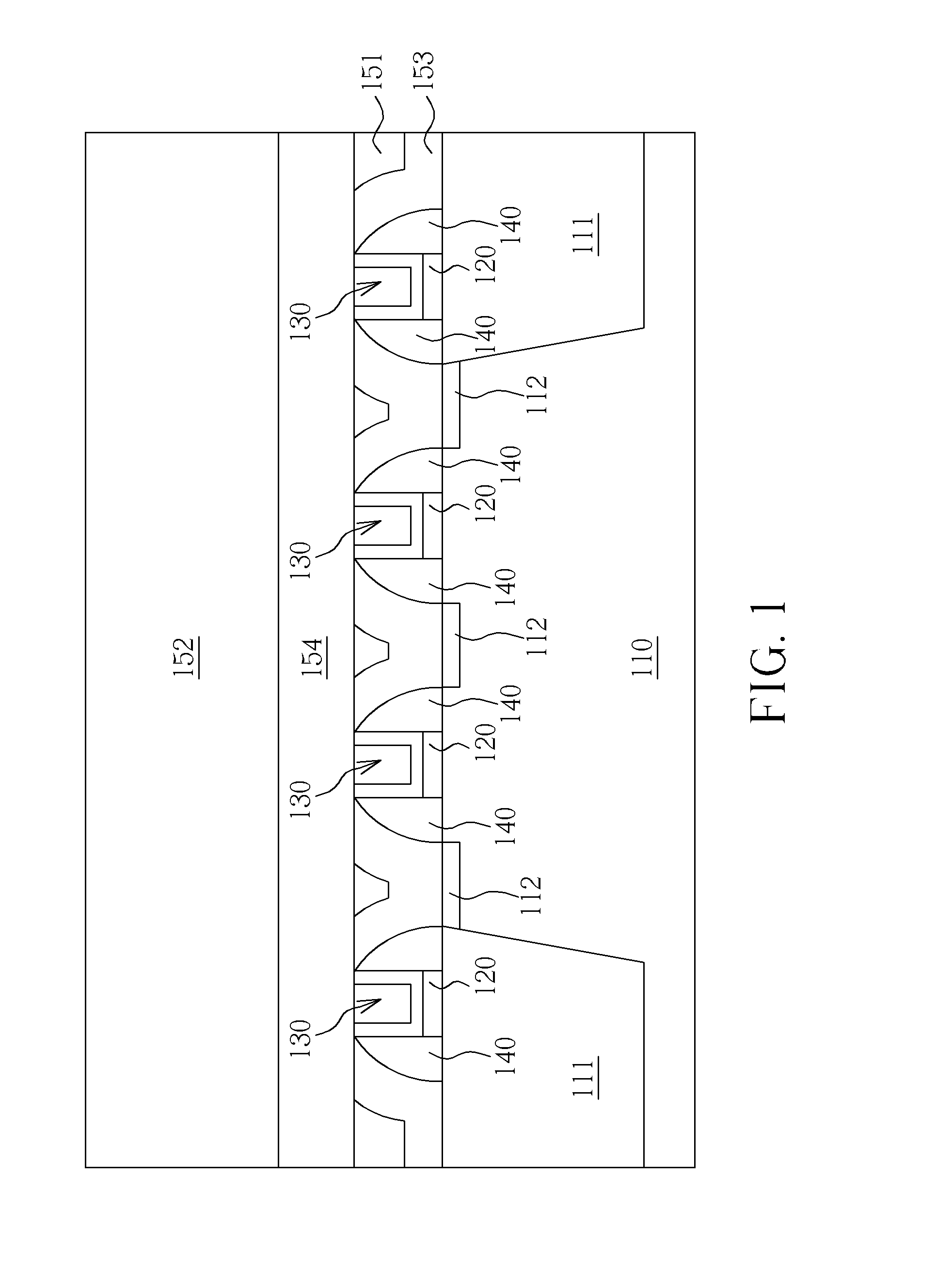
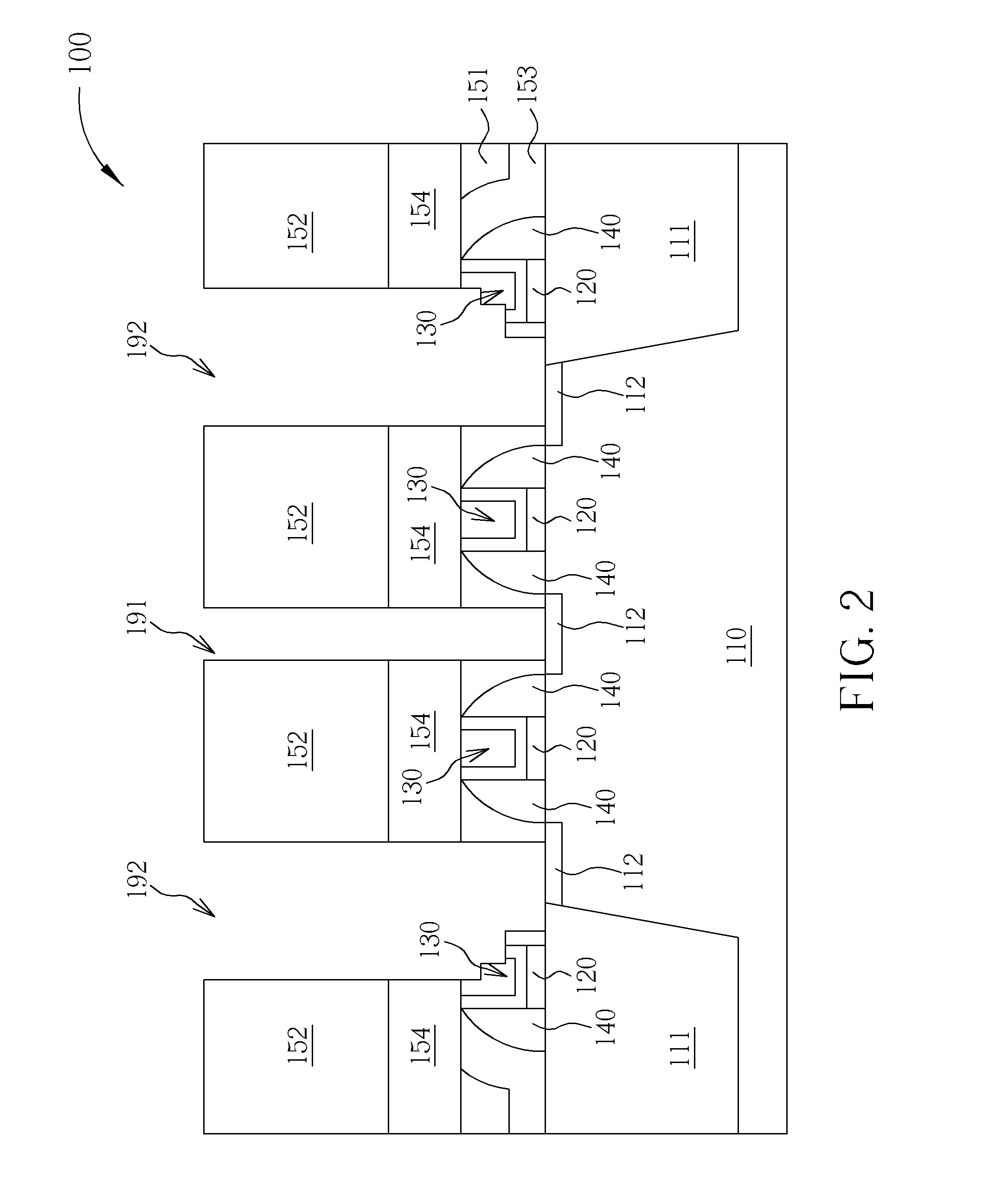
[0018]Please refer to FIG. 1 and FIG. 2. FIG. 1 and FIG. 2 are schematic diagrams illustrating a manufacturing method of the semiconductor device according to the first preferred embodiment of the present invention. Please note that the figures are only for illustration and the figures may not be to scale. The scale may be further modified according to different design considerations. The manufacturing method of the semiconductor device in this embodiment includes the following steps. First, as shown in FIG. 1, a substrate 110 is provided. A plurality of metal gate structures 130 are formed on the substrate 110. A plurality of diffusion regions 112, which may be used as source / drain electrodes, are formed in the substrate 110 at each of two sides of the metal gate structure 130 respectively. A plurality of spacers 140 are formed at each of the two sides of the metal gate structure 130 respectively. A plurality of gate dielectric layers 120 are disposed respectively between the subst...


PUM


Abstract

A manufacturing method of a semiconductor device includes the following steps. First, a substrate is provided. At least one sacrificial gate structure is formed on the substrate, at least one diffusion region is formed in the substrate at each of two sides of the sacrificial gate structure, and a first inter-layer dielectric layer is formed to cover the diffusion region. A gate recess is then formed in the sacrificial gate structure. A first diffusion contact hole is then formed in the first inter-layer dielectric layer and at least partially exposes the diffusion region. A metal layer is subsequently formed in the gate recess and the first diffusion contact hole.

Description

BACKGROUND OF THE INVENTION[0001]1. Field of the Invention[0002]The present invention relates to a semiconductor device and a manufacturing method thereof, and more particularly, to a semiconductor device and a manufacturing method thereof forming a contact hole on a diffusion region before forming a metal gate structure.[0003]2. Description of the Prior Art[0004]Poly-silicon is conventionally used as a gate electrode in semiconductor devices, such as the metal-oxide-semiconductor (MOS). With the trend towards scaling down the size of semiconductor devices, however, conventional poly-silicon gates face problems such as inferior performance due to boron penetration and unavoidable depletion effect. This increases equivalent thickness of the gate dielectric layer, reduces gate capacitance, and worsens a driving force of the devices. Therefore, work function metals that are suitable for use as the high dielectric constant (high-k) gate dielectric layer are used to replace the conventio...

Claims


Application Information

Patent Timeline
Patent Type & Authority Applications(United States)
IPC IPC(8): H01L27/092H01L21/768H01L29/78H01L21/28
CPCH01L29/66545H01L21/76895H01L21/76897H01L23/485H01L21/76843H01L21/76865H01L2924/0002H01L21/823437H01L29/665H01L29/78H01L2924/00
Inventor LEE, CHIU-TECHIOU, CHUN-MAOJHANG, YOU-DI
Owner UNITED MICROELECTRONICS CORP
Why Eureka
Try Eureka