High efficiency electro-static chucks for semiconductor wafer processing

a technology of electro-static chucks and semiconductor wafers, applied in the direction of chucks, turning machine accessories, packaging, etc., can solve the problems of limiting the lifetime of the chuck in certain substrate fabrication processes, oxygen-containing gases and plasmas, and affecting the polyimide layer of the electro-static chuck

Active Publication Date: 2009-08-13
APPLIED MATERIALS INC
View PDF11 Cites 12 Cited by
  • Summary
  • Abstract
  • Description
  • Claims
  • Application Information

AI Technical Summary

Problems solved by technology

However, the use of polyimide to insulate the electrode limits the lifetime of the chuck in certain substrate fabrication processes.
Oxygen-containing gases and plasmas, which are used for a variety of substrate processing operations, are particularly detrimental to the polyimide layers on the electrostatic chuck.
During these processes, the insulator can be eroded by the process gas and the resultant exposure of the electrode results in failure of the chuck during processing and loss of the entire substrate at a significant cost.
In addition, when a substrate breaks or chips to form fragments having sharp edges, the substrate fragments can easily puncture the polyimide film exposing the electrode of the chuck.
Exposure of the electrode at even a single pinhole in the insulator can cause arcing between the electrode and plasma, and require replacement of the entire chuck.
Further, the process of manufacturing the aforementioned electrostatic chuck requires the use of pressure or heat sensitive adhesives as well as a laborious circuit buildup.
This process is not only complicated, requiring many steps and extended fabrication time, but the adhesive layers may also be detrimentally affected by process conditions within certain process chambers.
This may result in delamination of the layers, requiring replacement of the entire chuck.

Method used


Image

  • High efficiency electro-static chucks for semiconductor wafer processing
  • High efficiency electro-static chucks for semiconductor wafer processing
  • High efficiency electro-static chucks for semiconductor wafer processing

Examples


Embodiment Construction

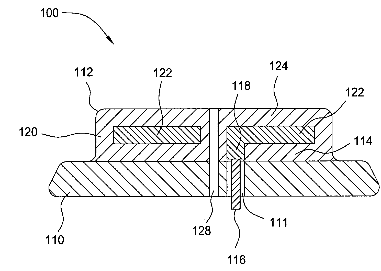
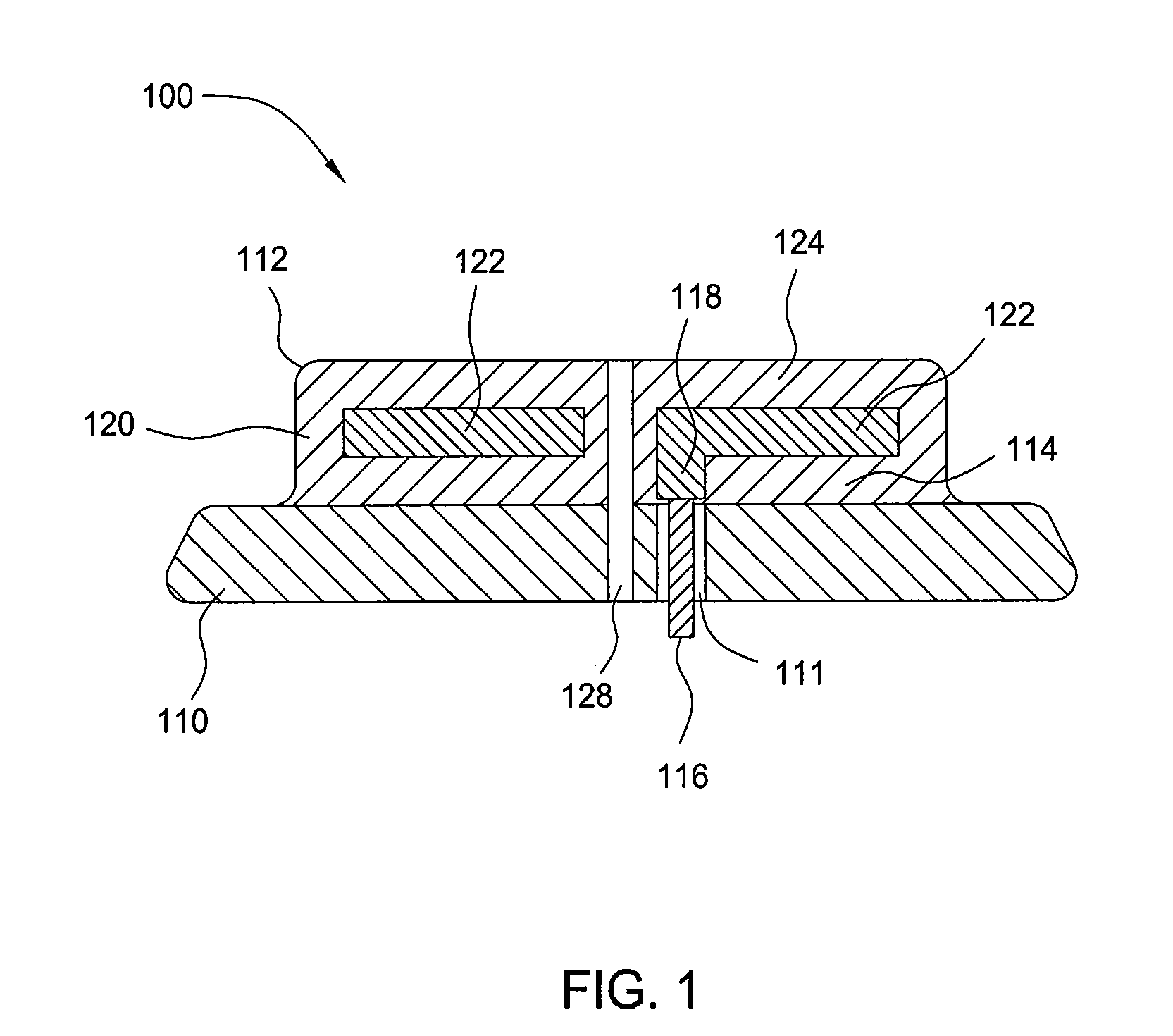
[0017]The present invention generally provides a high efficiency electrostatic chuck for holding a substrate in a processing volume. The high efficiency electrostatic chuck includes an electrode embedded between two layers of a high-purity, thermoplastic film. In particular, the high-purity, thermoplastic film may be a high-purity polyaryletherketone having an extremely low level of metallic ions present therein. High-purity polyaryletherketone has excellent wear resistance, high temperature resistance, plasma resistance, corrosive chemical resistance, electrical stability, and strength as compared to polyimide films currently used in electrostatic chucks. The present invention also provides a simplified method of manufacturing the high efficiency electrostatic chuck.

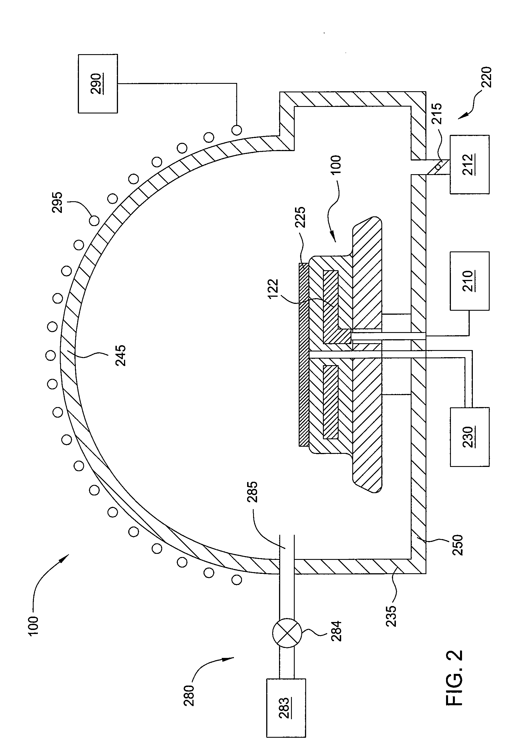
[0018]FIG. 1 is a schematic, cross-sectional view of an embodiment of an electrostatic chuck assembly 100 according to the present invention. The electrostatic chuck assembly 100 includes an electrostatic chuck 112 atop...


PUM

PropertyMeasurementUnit
surface areaaaaaaaaaaa
temperatureaaaaaaaaaa
voltageaaaaaaaaaa

Abstract

The present invention generally provides a high efficiency electrostatic chuck for holding a substrate in a processing volume. The high efficiency electrostatic chuck includes an electrode embedded within a high-purity, thermoplastic member. In particular, the high-purity, thermoplastic member may include a high-purity, polyaryletherketone having an extremely low level of metallic ions present therein. The high-purity, polyaryletherketone has excellent wear resistance, high temperature resistance, plasma resistance, corrosive chemical resistance, electrical stability, and strength as compared to polyimide films used in electrostatic chucks. The present invention also provides a simplified method of manufacturing the high efficiency electrostatic chuck.

Description

BACKGROUND OF THE INVENTION[0001]1. Field of the Invention[0002]Embodiments of the present invention generally relate to electrostatic chucks for holding a substrate in a process environment.[0003]2. Description of the Related Art[0004]In substrate processing applications, chucks are used to hold a substrate to prevent movement or misalignment of the substrate during processing. Electrostatic chucks use electrostatic attraction forces to hold a substrate in position. The use of electrostatic chucks has gained wide acceptance due to their advantages over mechanical and vacuum chucks, such as the reduction of stress related cracking in the substrate, the reduction of contamination in the processing chamber, and the ability to retain a substrate in a low vacuum environment.[0005]A typical electrostatic chuck includes an electrically conductive electrode embedded within an electrical insulator. A voltage source electrically biases the substrate with respect to the electrode. The insulat...

Claims


Application Information

Patent Timeline
Patent Type & Authority Applications(United States)
IPC IPC(8): B05C13/00B29C65/00
CPCB29C66/71B29K2071/00B29K2077/00B29K2101/12B29K2995/0006B29K2995/001Y10T156/10C23C16/4584H01L21/67017H01L21/67103H01L21/6831H01L21/6833Y10T279/23C23C14/505
Inventor BHATNAGAR, ASHISH
Owner APPLIED MATERIALS INC
Why Eureka
Try Eureka