Variable resistive element, and its manufacturing method

a resistive element and variable technology, applied in the direction of diodes, semiconductor devices, electrical apparatus, etc., to achieve the effect of stable switching operation and reduced current consumption

Active Publication Date: 2009-08-13
XENOGENIC DEV LLC
View PDF20 Cites 56 Cited by
  • Summary
  • Abstract
  • Description
  • Claims
  • Application Information

AI Technical Summary

Benefits of technology

[0078]According to the variable resistive element of the present invention, an area of an electrically contributing region of a variable resistor body is not to be constrained by a formative area specified by manufacturing processes, because a shape of a contact surface of between the variable resistor body and either one of electrodes or the other one of the electrodes is an annular or a plurally-separated linear shape. Hence, it becomes able to obtain the area of the electrically contributing region of the variable resistor body smaller than the formative area specified by the manufacturing processes. Therefore, it becomes able to reduce the current consumption at a period of programming or erasing thereby, and then it becomes able to manufacture a memory element reproducibly with a stable switching operation without occurring a programming impossible due to a low electrical resistance thereof. Moreover, according to the manufacturing method for a variable resistive element regarding the present invention, it becomes able to manufacture such as the above mentioned variable resistive element which is able to obtain the area of the electrically contributing region of the variable resistor body smaller than the formative area specified by the manufacturing processes.

Problems solved by technology

However, each of such the current memory devices has both advantages and disadvantages respectively, and it is still a long way away from realizing an ideal universal memory having every advantage of a static RAM (SRAM), a dynamic RAM (DRAM) and the flash memory.

Method used


Image

  • Variable resistive element, and its manufacturing method
  • Variable resistive element, and its manufacturing method
  • Variable resistive element, and its manufacturing method

Examples


first embodiment

The First Embodiment

[0164]The first embodiment according to the present invention element and the present invention method (properly referred to as the present embodiment hereinafter) will be described in detail below with reference to FIG. 1 to FIG. 5.

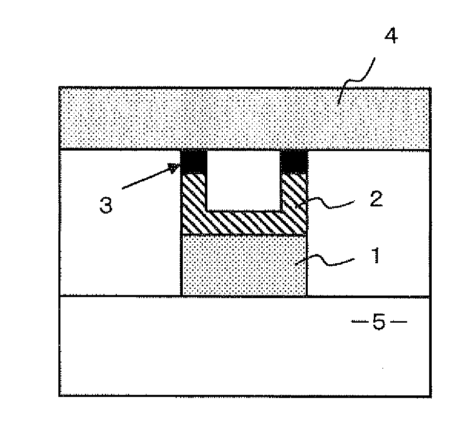
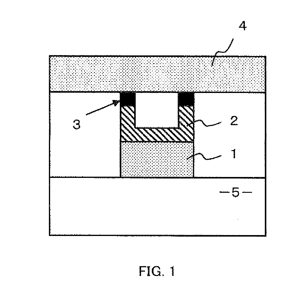
[0165]FIG. 1 is a brief cross sectional view showing the present invention element according to the present embodiment. The present invention element according to the present embodiment comprises a configuration that a lower electrode wiring 1 and an upper electrode wiring 4 are formed on a base substrate 5, and a variable resistor body 3 as a memory material body is formed between the upper and the lower electrode wirings, wherein a bump electrode material 2 comprised of any of electrically conductive materials is electrically connected to the lower electrode wiring 1, and the variable resistor body 3 is formed on an apical part of the bump electrode material 2, as shown in FIG. 1.

[0166]The following is a description as an example fo...

second embodiment

The Second Embodiment

[0182]The second embodiment according to the present invention element and the present invention method (properly referred to as the present embodiment hereinafter) will be described in detail below with reference to FIG. 6 to FIG. 9. Here, a detailed description for a process which duplicates that of the first embodiment is properly omitted with mentioning that effect.

[0183]Moreover, the description as a first insulating film or a second insulating film is named for an insulating film for convenience' sake in order of depositing thereof for each of the embodiments, and it is to be used independently for each of the embodiment except a case of mentioning in particular. Ditto regarding each of the following embodiments.

[0184]FIG. 6 is a cross sectional pattern diagram showing the present invention element according to the present embodiment. The present invention element according to the present embodiment comprises a configuration that a lower electrode wiring 3...

third embodiment

The Third Embodiment

[0198]The third embodiment according to the present invention element and the present invention method (properly referred to as the present embodiment hereinafter) will be described in detail below with reference to FIG. 10 and FIG. 11. Here, a detailed description for a process which duplicates that of the first embodiment is properly omitted with mentioning that effect.

[0199]According to the above mentioned first and the second embodiment, the variable resistor body is formed by oxidizing the bump electrode material, however, the present invention element is to be formed using a method for depositing a variable resistor body directly onto a bump electrode material according to the present embodiment. The following is a description as an example for the case of applying the manufacturing method for a variable resistive element according to the present embodiment to a memory cell of 1R type.

[0200]FIG. 10 and FIG. 11 are views showing manufacturing processes for t...


PUM


Abstract

A variable resistive element comprising a configuration that an area of an electrically contributing region of a variable resistor body is finer than that constrained by an upper electrode or a lower electrode and its manufacturing method are provided. A bump electrode material is formed on a lower electrode arranged on a base substrate. The bump electrode material is contacted to a variable resistor body at a surface different from a contact surface to the lower electrode. The variable resistor body is contacted to an upper electrode at a surface different from a contact surface to the bump electrode material. Thus, a cross point region between the bump electrode material (the variable resistor body) and the upper electrode becomes an electrically contributing region of the variable resistor body, and then an area thereof can be reduced compared with that of the region regarding the conventional variable resistive element.

Description

CROSS-REFERENCE TO RELATED APPLICATIONS[0001]This application is a National Phase filing under 35 U.S.C. § 371 of International Application No. PCT / JP2007 / 053358 filed on Feb. 23, 2007, and which claims priority to Japanese Patent Application No. 2006-125432 filed on Apr. 28, 2006.TECHNICAL FIELD[0002]The present invention relates to a variable resistive element comprising an electrode, another electrode and a variable resistor body, wherein the variable resistor body is provided between the one electrode and the other electrode, and an electrical resistance of the variable resistive element is changed by applying a voltage pulse between both of the electrodes, and relates to its manufacturing method.BACKGROUND ART[0003]In recent years, a variety of device structures are presented, such as a ferroelectric random access memory (FeRAM), a magnetic RAM (MRAM), a phase change RAM (PRAM), or the like, as a next generation nonvolatile RAM (NVRAM) for fast operation possible taking the pla...

Claims


Application Information

Patent Timeline
Patent Type & Authority Applications(United States)
IPC IPC(8): H01L29/8605H01L21/02H01L45/00
CPCH01L27/101H01L45/16H01L45/04H01L45/1226H01L45/1233H01L45/124H01L45/1273H01L45/146H01L45/1616H01L45/1625H01L45/1633H01L45/1691H01L27/2436H01L27/2463H01L45/1253H01L45/145H10B63/30H10B63/80H10N70/20H10N70/8265H10N70/823H10N70/8418H10N70/883H10N70/028H10N70/023H10N70/068H10N70/026H10N70/8833H10N70/826H01L27/10H01L28/00H10N70/00H10N99/00H10N70/841H10N70/011
Inventor HOSOI, YASUNARIISHIHARA, KAZUYASHIBUYA, TAKAHIROOHNISHI, TETSUYANAKANO, TAKASHI
Owner XENOGENIC DEV LLC
Why Eureka
Try Eureka