Wiring substrate for use in semiconductor apparatus, method for fabricating the same, and semiconductor apparatus using the same

a technology for wiring substrates and semiconductor apparatuses, applied in the direction of electrical apparatus construction details, resist details, fixed connections, etc., can solve the problems of metal thin wire separation, metal thin wire deformation, and uncleanness and/or deformation of metal thin wires, so as to reduce unevenness

Active Publication Date: 2009-08-13
PANASONIC SEMICON SOLUTIONS CO LTD
View PDF8 Cites 11 Cited by
  • Summary
  • Abstract
  • Description
  • Claims
  • Application Information

AI Technical Summary

Benefits of technology

[0013]Therefore, an object of the present invention is to provide, for solving the problems described above, a wiring substrate for use in a semiconductor apparatus having such a stable quality as to suppress generation of bubbles (voids) between a semiconductor chip and the wiring substrate for use in the semiconductor apparatus, and prevent separation betw

Problems solved by technology

There is a problem that, in the process of fabricating a semiconductor apparatus, a contact between the applied solder resist and a solder resist of a bonding tool (capillary) used for connection (wire bonding) of the metal thin wire causes uncleanness and/or deformation of the metal thin wire.
However, in the conventional wiring substrate for use in the semiconductor apparatus, unevenness is increased due to the vias and wirings in an area in which the semiconductor chip is mounted, and therefore b

Method used


Image

  • Wiring substrate for use in semiconductor apparatus, method for fabricating the same, and semiconductor apparatus using the same
  • Wiring substrate for use in semiconductor apparatus, method for fabricating the same, and semiconductor apparatus using the same
  • Wiring substrate for use in semiconductor apparatus, method for fabricating the same, and semiconductor apparatus using the same

Examples


first embodiment

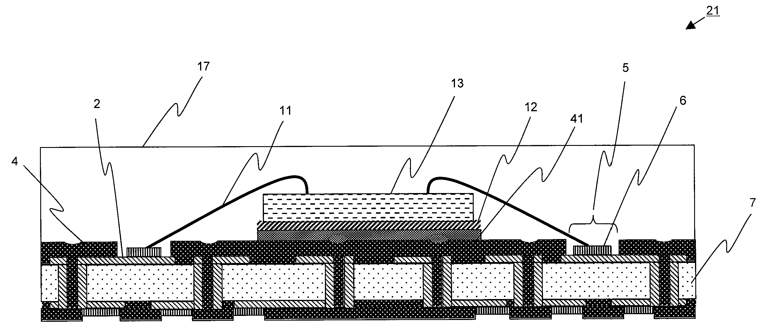
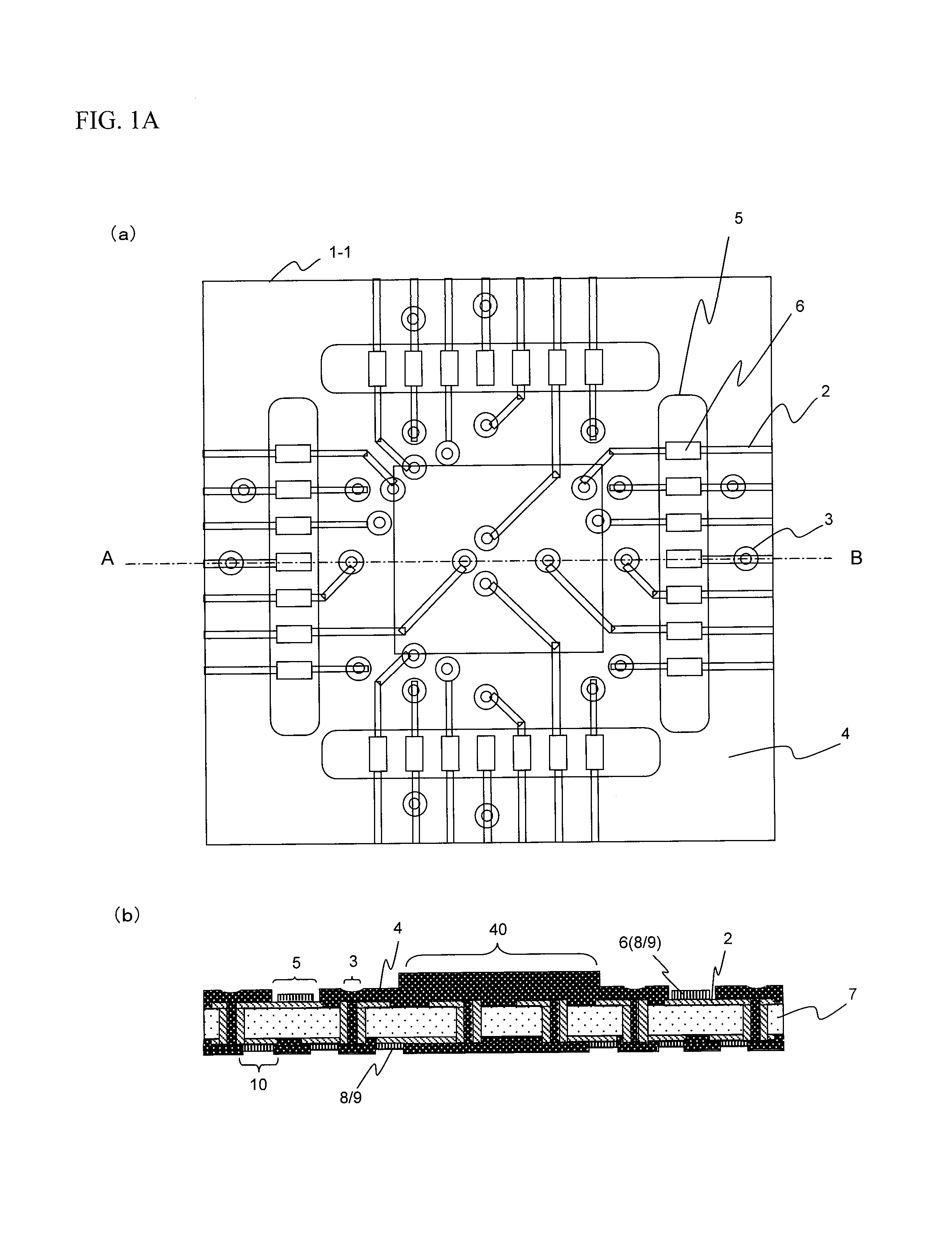
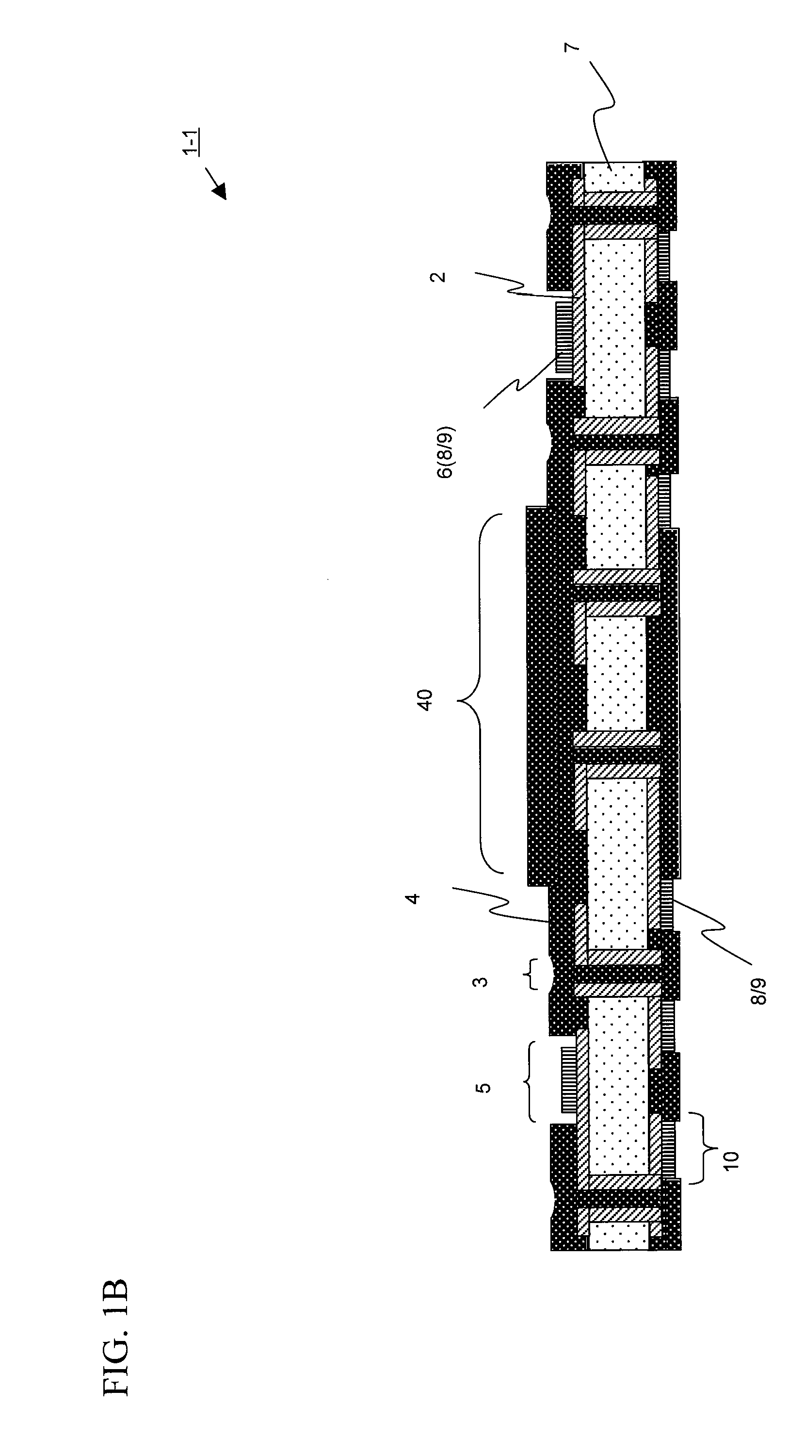
[0047]FIG. 1A is a diagram illustrating a printed-wiring board 1-1 which is a wiring substrate for use in a semiconductor apparatus according to a first embodiment of the present invention. FIG. 1A(a) is atop view of the printed-wiring board 1-1. In FIG. 1A(a), the printed-wiring board 1-1 is patterned with a conductor layer 2, and the conductor layer 2 is electrically connected through vias 3 to a conductor layer which is provided on the bottom surface of the printed-wiring board 1-1. On a bonding pad positioning area 5 of the printed-wiring board 1-1, a bonding pad 6 is positioned so as to connect to the conductor layer 2, and a surface portion of each of the bonding pad 6 and the conductor layer 2 is Ni / Au-plated. A solder resist 4 is applied to portions other than the bonding pad positioning area 5 of the printed-wiring board 1-1. A configuration of the top surface of the printed-wiring board 1-1 is the same as the configuration of the conventional printed-wiring board 101 shown...

second embodiment

[0057]FIG. 5 is a diagram illustrating a printed-wiring board 1-2 which is a wiring substrate for use in a semiconductor apparatus according to a second embodiment of the present invention. FIG. 5(a) is a top view of the printed-wiring board 1-2, and FIG. 5(b) is a cross-sectional view of the printed-wiring board 1-2 shown in FIG. 5(a) along lines A-B. A configuration of the printed-wiring board 1-2 is almost the same as the configuration of the printed-wiring board 1-1 according to the first embodiment of the present invention, and, in FIG. 5, components which are the same or correspond to those shown in FIG. 1A are denoted by the same corresponding reference numerals, and the description thereof is not given. In the present embodiment, difference between the printed-wiring board 1-2 and the printed-wiring board 1-1 will be described in detail.

[0058]As shown in FIG. 1A, in the printed-wiring board 1-1 according to the first embodiment of the present invention, the solder resist 4 f...

third embodiment

[0067]FIG. 8 is a diagram illustrating a printed-wiring board 1-3 which is a wiring substrate for use in the semiconductor apparatus according to a third embodiment of the present invention. FIG. 8(a) is a top view of the printed-wiring board 1-3, and FIG. 8(b) is a cross-sectional view of the printed-wiring board 1-3 shown in FIG. 8(a) along lines A-B. A configuration of the printed-wiring board 1-3 is almost the same as each of the configuration of the printed-wiring board 1-1 according to the first embodiment of the present invention and the configuration of the printed-wiring board 1-2 according to the second embodiment of the present invention, and, in FIG. 8, components which are the same or correspond to those shown in FIG. 1A and FIG. 5 are denoted by the same corresponding reference numerals, and the description thereof is not given. In FIG. 8(b), the printed-wiring board 1-3 is different from the printed-wiring board 1-1 and the printed-wiring board 1-2 in that the printed...


PUM


Abstract

On a printed-wiring board 1-1, a conductor layer 2 is laminated to both the top surface and the bottom surface of a substrate core 7 so as to pattern the substrate core, and a solder resist 4 is laminated to the substrate core. The solder resist 4 laminated to the top surface of the printed-wiring board 1-1 forms a raised portion 40 in a semiconductor chip mounting area such that the thickness of the raised portion is greater than the thickness of the solder resist 4 laminated to areas other than the semiconductor chip mounting area, so that the surface of the semiconductor chip mounting area is flat.

Description

BACKGROUND OF THE INVENTION[0001]1. Field of the Invention[0002]The present invention relates to a wiring substrate and a method for fabricating the wiring substrate, and more particularly to a wiring substrate for use in a semiconductor apparatus such as a BGA, and a method for fabricating the wiring substrate.[0003]2. Description of the Background Art[0004]In recent years, an electronic apparatus not only has its size and thickness reduced but also has its performance enhanced and its function diversified. In order to realize specifications of the electronic apparatus, a semiconductor apparatus, which is the most important component for the electronic apparatus, tends to have its size and thickness reduced, and further include the increased number of terminals. Under these situations, as a configuration of the semiconductor apparatus, a so-called BGA (Ball Grid Array) package, LGA (Land Grid Array) package, and the like are generally known. The BGA package and the LGA package incl...

Claims


Application Information

Patent Timeline
IPC IPC(8): H01R12/06H01L23/12H01B13/00H01R12/51
CPCH01L23/49822H01L23/49838H01L2224/83192H05K2201/2036H01L2924/01033H01L2924/01006H01L24/32H05K2203/0588H05K2203/049H05K3/3452H01L2924/15173H01L2924/014H01L2924/01082H01L2924/01079H01L2924/01078H01L2924/01029H01L2924/01028H01L2924/01015H01L2924/01005H01L24/45H01L24/48H01L24/83H01L2224/32225H01L2224/45144H01L2224/48091H01L2224/48227H01L2224/48228H01L2224/484H01L2224/48599H01L2224/73265H01L2224/838H01L2224/85444H01L2224/92247H01L2924/01004H01L2924/00014H01L2924/00H01L2924/00012H01L24/73H01L2224/48644H01L2924/181
Inventor TANAKA, HIROYUKISUZUKI, HIROAKI
Owner PANASONIC SEMICON SOLUTIONS CO LTD
Why Eureka
Try Eureka