
Non binary flash array architecture and method of operation

a non-binary, flash array technology, applied in the direction of read-only memories, instruments, static storage, etc., can solve the problems of device failure to work reliably, device failure to erase operations, and loss of anything contained in ram, so as to improve layout efficiency

Active Publication Date: 2009-08-13
SPANSION ISRAEL
View PDF21 Cites 14 Cited by
  • Summary
  • Abstract
  • Description
  • Claims
  • Application Information

AI Technical Summary

Benefits of technology

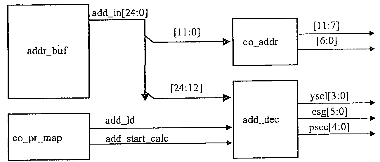
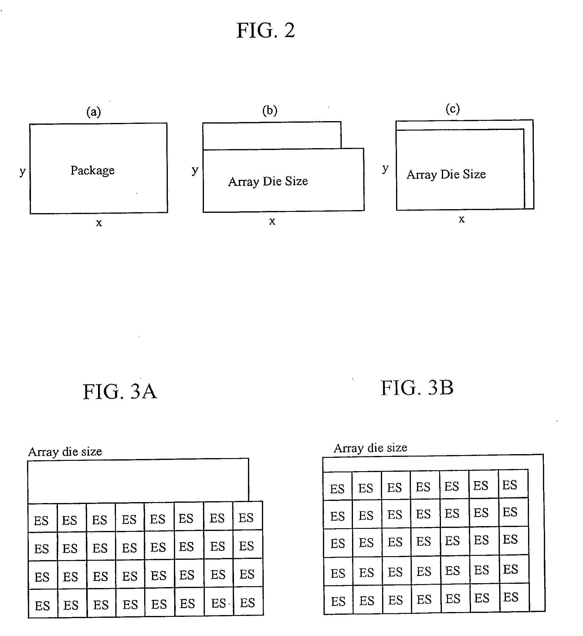
[0061]According to the disclosure, generally, a non volatile memory (NVM) array, such as a Flash memory array may be implemented with a non-binary number of Physical Sectors (PSecs), Physical Pages (slices) and / or Erase Sector Groups (ESGs). This may improve layout efficiency. (There may also be a non-binary number of wordlines per Erase Sector Group.) Techniques for converting (typically) binary user addresses to the non-binary physical addresses are disclosed.

Problems solved by technology

However, an erase operation is not mandatory for a Flash memory.
NOR flash chips lack intrinsic bad block management, so when a flash block is worn out, the software or device driver controlling the device must handle this, or the device will cease to work reliably.
The most widely used form of primary storage today is a volatile form of random access memory (RAM), meaning that when the computer is shut down, anything contained in RAM is lost.
Unfortunately most forms of non-volatile memory have limitations which make it unsuitable for use as primary storage.
Typically non-volatile memory either costs more or performs worse than volatile random access memory.

Method used


Image

  • Non binary flash array architecture and method of operation
  • Non binary flash array architecture and method of operation
  • Non binary flash array architecture and method of operation

Examples


Embodiment Construction

[0079]In the following description, various aspects of techniques for implementing and operating a Flash memory array will be described. For the purpose of explanation, specific configurations and details are set forth in order to provide a thorough understanding of the techniques. However, it will also be apparent to one skilled in the art that the techniques may be practiced without specific details being presented herein. Furthermore, well-known features may be omitted or simplified in order not to obscure the description(s) of the techniques.

[0080]Throughout the descriptions set forth in this disclosure, lowercase numbers or letters may be used, instead of subscripts. For example Vg could be written Vg. Generally, lowercase is preferred to maintain uniform font size.) Regarding the use of subscripts (in the drawings, as well as throughout the text of this document), sometimes a character (letter or numeral) is written as a subscript—smaller, and lower than the character (typical...


PUM


Abstract

A Flash memory array comprises a plurality of Erase Sectors (Esecs) arranged in a plurality of Erase Sector Groups (ESGs), Physical Pages (slices), and Physical Sectors (PSecs), and there is a non-binary number of at least one of the Erase Sector Groups (ESGs), Physical Pages (slices), and Physical Sectors (PSecs). A user address is translated into a physical address using modular arithmetic to determine pointers (ysel, esg, psec) for specifying a given Erase Sector (ESec) within a given Erase Sector Group (ESG); a given Erase Sector Group (ESG) within a given Physical Sector (Psec); and a given Physical Sector (PSec) within the array.

Description

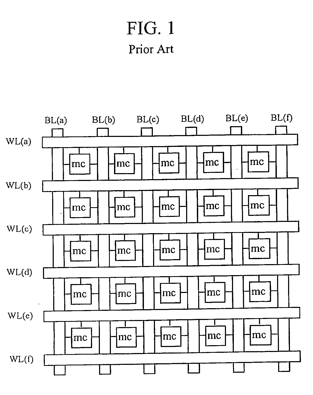
CROSS-REFERENCE(S) TO RELATED APPLICATION(S)[0001]This application claims priority from U.S. Provisional Patent Application No. 60 / 984,402 filed Nov. 1, 2007 which is hereby incorporated by reference in its entirety.TECHNICAL FIELD[0002]The disclosure relates to semiconductor devices and, more particularly, to techniques for implementing and operating non-volatile memory (NVM), such as floating gate (FG) devices or charge-trapping devices such as nitride read only memory (NROM) devices, or other microelectronic cells or structures.BACKGROUND[0003]Memory arrays are well known, and comprise a plurality (many, including many millions) of memory cells organized (including physically arranged) in rows (usually represented in drawings as going across the page, horizontally, from left-to-right) and columns (usually represented in drawings as going up and down the page, from top-to-bottom).[0004]FIG. 1 illustrates an exemplary, generic memory array. A plurality of bitlines, labeled BL(a) th...

Claims


Application Information

Patent Timeline
Patent Type & Authority Applications(United States)
IPC IPC(8): G06F12/00G11C11/34G11C8/00G06F12/02
CPCG06F12/0246G11C16/16G06F2212/7206
Inventor LAVAN, AVISHAHAR, RAN
Owner SPANSION ISRAEL
Learn More