Automated Method and Apparatus for Very Early Validation of Chip Power Distribution Networks in Semiconductor Chip Designs

a technology of chip power distribution network and chip design, applied in computer aided design, program control, instruments, etc., can solve problems such as inability to identify new power distribution problems, easy to connect to the chip power grid, and often susceptible to connectivity issues, so as to speed up the checking algorithm and quickly identify new power connection problems

Inactive Publication Date: 2009-08-20
GLOBALFOUNDRIES INC
View PDF37 Cites 6 Cited by
  • Summary
  • Abstract
  • Description
  • Claims
  • Application Information

AI Technical Summary

Benefits of technology

[0029]Another objective of the invention is to enable early checking results and to speed up checking algorithms, by using early design information that already exists in the chip power grid and the chip floor pl

Problems solved by technology

As a chip floor plan evolves over time, a chip power grid becomes susceptible to connectivity issues.
A minor change in circuit placement, a circuit's reserved metal blockage, or a circuit's power image may result in new power distribution problems.
Unfortunately, such issues are often not identified until full-chip physical design (PD) checks are performed.
However, complete re-implementation of full-chip power grid for designs that are already in controlled engineering change (EC) mode is usually not desired, as this action may result in changes that may require design re-qualifications beyond the original intended circuit's EC.
Both the logical and the physical chip netlists are ty

Method used


Image

  • Automated Method and Apparatus for Very Early Validation of Chip Power Distribution Networks in Semiconductor Chip Designs
  • Automated Method and Apparatus for Very Early Validation of Chip Power Distribution Networks in Semiconductor Chip Designs
  • Automated Method and Apparatus for Very Early Validation of Chip Power Distribution Networks in Semiconductor Chip Designs

Examples


Embodiment Construction

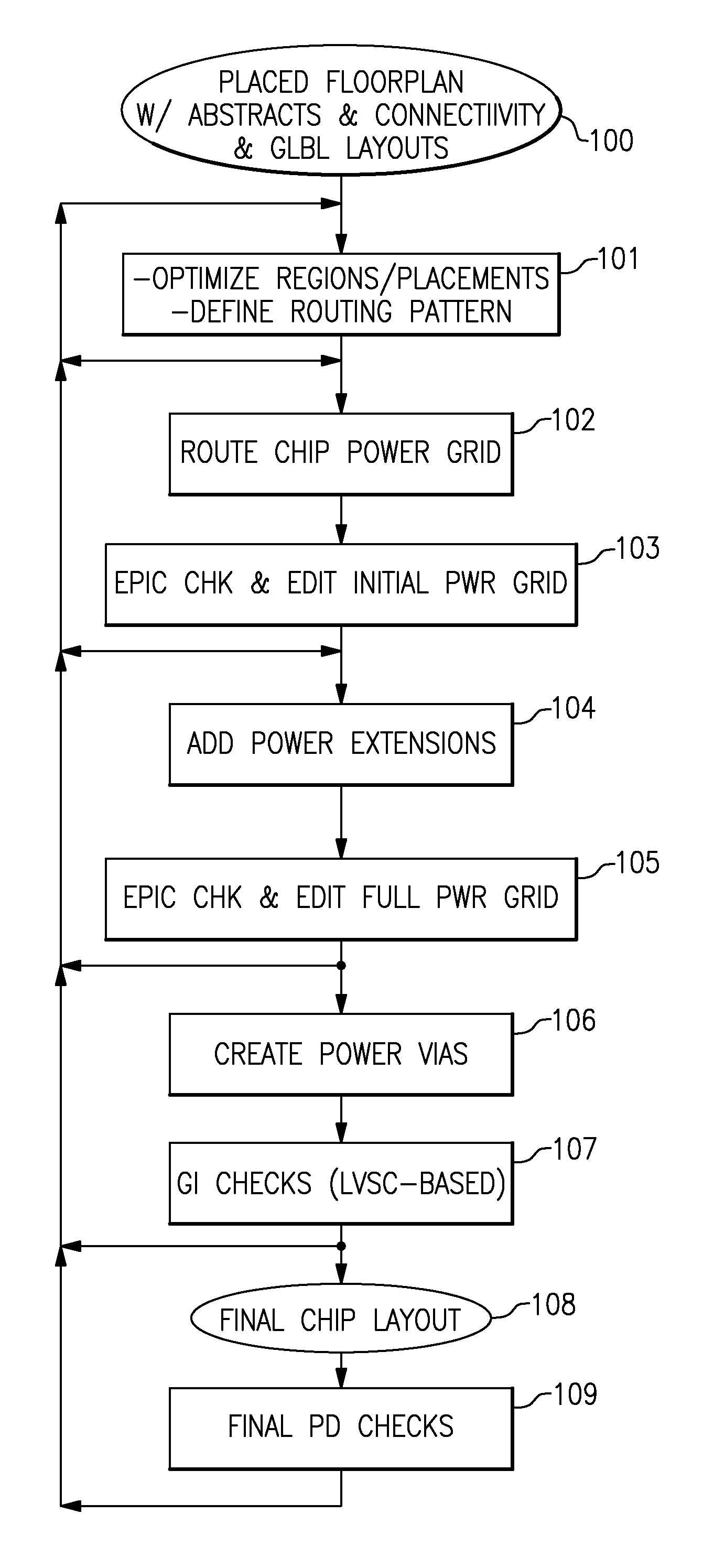
[0038]FIG. 1 illustrates an enhanced chip power routing and verification process, which uses the invention's EPIC toolset to validate early versions of the chip power grid. As described in the above-identified co-pending application Ser. No. (POU920070243), a chip floor plan 100 is generated from circuit abstracts and a circuit net list. Full-chip power routing of all metals 102 typically starts after timing-driven placements and power routing controls are defined 101 for the given input chip floor plan 100. Certain EPIC checking functions 103 are meant to be used early in the design process to highlight possible improvements in the chip floor plan and / or in this initial chip power grid. For instance, a power shorting to a circuit abstract may result in a circuit placement change or a power routing pattern change. Another example is to find all multi-power domain macros whose highest power metal pins have no accessibility to the initial chip power grid on either the same or the next...


PUM


Abstract

Validation of full-chip power distribution networks can be performed very early, and continuously throughout the design cycle, to detect real physical power connection problems and enable early correction of power grid designs using early floor plan and power grid design data. Common power connection and distribution errors are automatically addressed as an integral part of the early chip floor planning and chip power build processes providing efficient solutions requiring no extra wiring resource to be implemented and reducing the runtime of required final full-chip physical design checks, and the overall design cycle.

Description

CROSS-REFERENCE TO RELATED APPLICATIONS[0001]This application contains subject matter related to the following co-pending applications, each of which is assigned to the same assignee as this application, International Business Machines Corporation of Armonk, N.Y. Each of the below listed applications is hereby incorporated herein by reference in its entirety.[0002]Co-pending U.S. patent application Ser. No. 11 / 055,863 filed Feb. 11, 2005 and entitled “Method and Apparatus for Specifying Multiple Voltage Domains and Validity Physical Implementation and Interconnection in a Processor Chip.”[0003]U.S. patent application Ser. No. (IBM-POU920070243) filed on even date herewith and entitled “Method and Apparatus for Efficient Power Region Checking of Multi-Supply Voltage Microprocessors.”TRADEMARKS[0004]IBM® is a registered trademark of International Business Machines Corporation, Armonk, N.Y., U.S.A. Other names used herein may be registered trademarks, trademarks or product names of Int...

Claims


Application Information

Patent Timeline
IPC IPC(8): G06F17/50
CPCG06F2217/78G06F17/5081G06F30/398G06F2119/06
Inventor PHAN VOGEL, DIEU Q.
Owner GLOBALFOUNDRIES INC
Why Eureka
Try Eureka