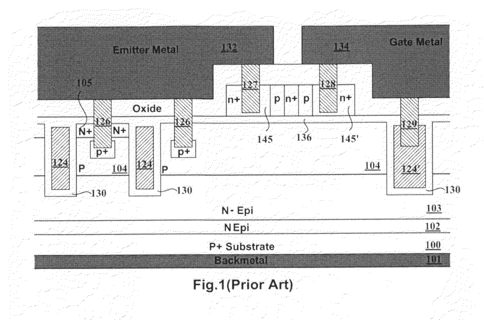
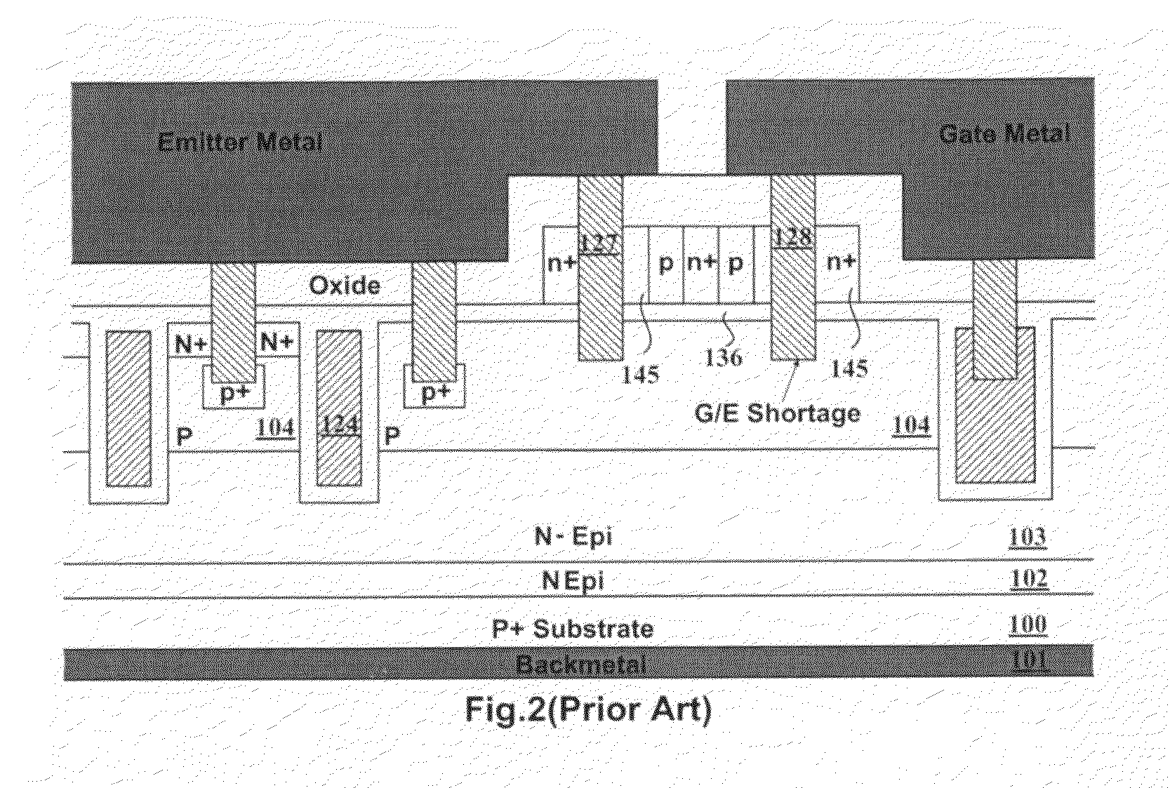
[0009]One
advantage of the present invention is that, additional trench gates are applied in lightly doped epitaxial layer right below trench contacts in ESD protection diodes. By employing this configuration, no shortage issue will happen even if over
etching takes place during manufacture process.
[0010]Another
advantage of the present invention is that, no additional cost is required to implement the trench gates underneath contact areas of protection diodes since the trench gates can be formed at the same step as other trench gates formed.
[0011]Another
advantage of the present invention is that, the inventive structure is suitable for both PT IGBT and NPT IGBT with G-C Clamp Diodes or with G-E Clamp Diodes or with G-C and G-E Clamp Diodes.
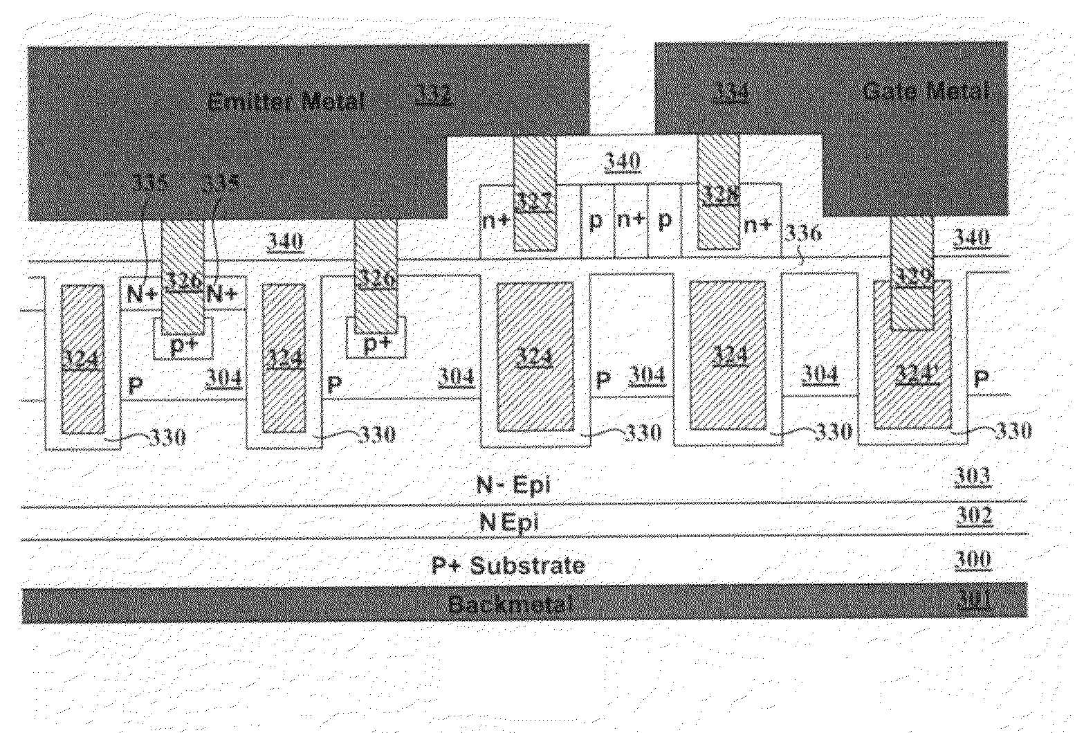
[0012]Briefly, in a preferred embodiment, as shown in FIG. 3B, the present invention discloses a trench PT IGBT
cell with G-E Clamp Diodes for G-E ESD protection. The
transistor cell comprises: a first epitaxial layer moderately doped with a first
semiconductor doping type (e.g., N
dopant) grown onto a substrate heavily doped with a second
semiconductor doping type (e.g., P
dopant) coated with a back
metal on its rear side; a second epitaxial layer lightly doped with the same
doping type as the first epitaxial layer and grown whereon; a plurality of trenches and at least a wider trench etched within the second epitaxial layer and filled with doped poly over a
gate oxide layer to form trench gates and at least a wider
trench gate for gate connection; base regions formed within the top portion of the second epitaxial layer and moderately doped with the opposite doping type to epitaxial layer; emitter regions heavily doped with the same doping type as the epitaxial layer near the front surface of base region between two adjacent trench gates; a doped polysilicon layer overlying a portion of the insulating layer as ESD protection diodes comprising multiple back to back Zener diodes which composed of doping areas of a first semiconductor doping type next to doping areas of a second semiconductor doping type; trench contacts penetrating through a thick
dielectric interlayer and emitter, and extending into base regions, two cathodes of ESD protection diodes, and at least a wider
trench gate to electrically connect the emitter regions, the base regions and one
cathode of ESD protection diodes to the emitter
metal, and to electrically connect the
trench gate and another
cathode of ESD protection diodes to the gate
metal, respectively; an area heavily doped with the same doping type as base region around each bottom of trench emitter contact and trench base contact to reduce
contact resistance between base region and metal plug filled in trench contacts. Specially, additional trench gates are formed right underneath each trench contact of the ESD protection diodes as a buffer layer to avoid G-E shortage issue.
[0013]Briefly, in another preferred embodiment, as shown in FIG. 4B, the present invention discloses a trench PT IGBT cell with G-C Clamp Diodes for G-C protection. Different from configuration in FIG. 3B, here one
cathode of the ESD protection diodes is connected to gate metal while another is connected to collector metal. However, despite all that, there are still inventive trench gates right underneath each trench contact of G-C protection diodes to ward off the happening of shortage issue between G-C, or G-E, or G-C-E resulted from trench contacts of ESD protection over
etching to base regions.
[0014]Briefly, in another preferred embodiment, as shown in FIG. 5B, the present invention discloses a trench PT IGBT cell with both G-E and G-C Clamp Diodes for G-E and G-C ESD protection, respectively. The pluralities of Zener Diodes contain at least three cathodes to be connected to gate metal, emitter metal and collector metal, respectively. Underneath each trench contact of protection diodes, a trench gate is formed to ward off the shortage of gate and collector to emitter resulted from trench contacts of ESD protection over etching to base regions.
