Methods for enhancing photolithography patterning

a technology of photolithography and patterning, applied in the field of photolithography processes, can solve the problems of unsuitable forbidden pitches, high dependence, and space is too small for scattering bars, and achieve the effects of improving process windows, improving process windows, and improving second pitches

Active Publication Date: 2009-08-27
NAT UNIV OF SINGAPORE +2
View PDF7 Cites 24 Cited by
  • Summary
  • Abstract
  • Description
  • Claims
  • Application Information

AI Technical Summary

Benefits of technology

[0010]In one aspect of the invention, there is provided a method for fabricating a semiconductor device comprising: providing a substrate prepared with a photoresist layer; providing a photomask comprising a first and a second pattern having a respective first and second pitch range; providing a composite aperture comprising a first and a second off-axis illumination aperture pattern, the first off-axis illumination aperture pattern having a configuration that improves the process window of the first pitch range and the second off-axis illumination aperture pattern having a configuration that improves the process window for a second pitch range; exposing t

Problems solved by technology

Forbidden pitches are undesirable as the critical dimension fluctuation prevents a circuit designer from being able to use the affected pitch range in his design.
However, one of the problems with the biasing approach is that it is highly dep

Method used


Image

  • Methods for enhancing photolithography patterning
  • Methods for enhancing photolithography patterning
  • Methods for enhancing photolithography patterning

Examples


Embodiment Construction

[0029]Generally, the present invention relates to photolithography processes that reduce variability in critical dimensions of photoresist structures caused by differences in proximity to other features.

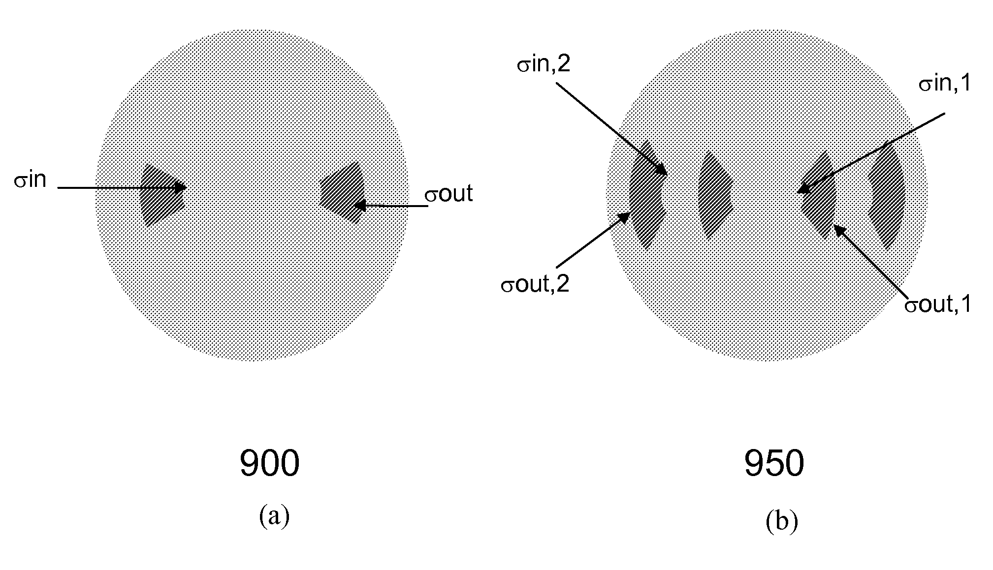
[0030]During an exposure process, the illumination beam can be projected onto a photomask from a number of different angles depending on the arrangement of the opening or openings on the aperture of an exposure tool. If aperture comprises an opening that is situated at the center of the aperture, the illuminating beam will be projected substantially along the optical axis, that is, the axis orthogonal to the condenser lens and photomask. This type of illumination is known as “On-axis illumination”.

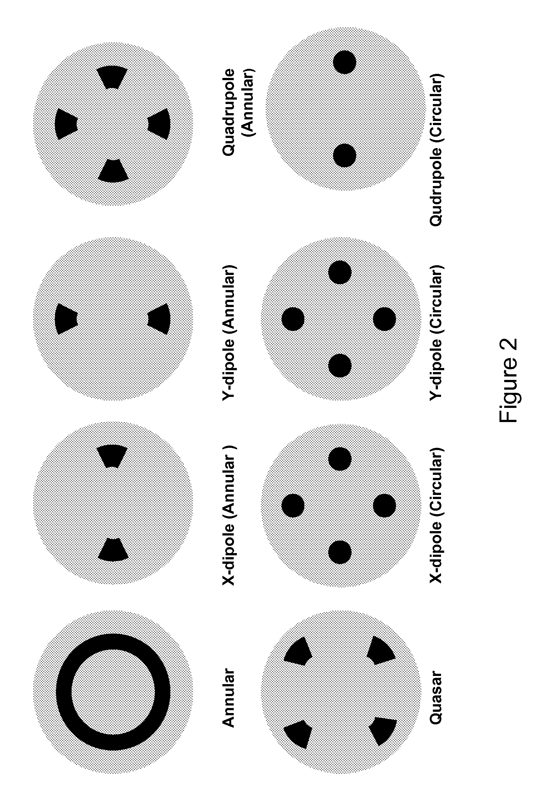
[0031]On the other hand, if the aperture is centrally obstructed and has one or more openings located off-center, the illumination beam is tilted projected onto the photomask away from normal incidence, in other words, at an angle to the optical axis. This type of illumination is referred t...


PUM


Abstract

A method for fabricating a a semiconductor device that includes: providing a substrate prepared with a photoresist layer; providing a photomask comprising a first and a second pattern having a respective first and second pitch range; providing a composite aperture comprising a first and a second off-axis illumination aperture pattern, the first off-axis aperture pattern having a configuration that improves the process window of the first pitch range and the second off-axis aperture pattern having a configuration that improves the process window for a second pitch range; exposing the photoresist layer on the substrate with radiation from an exposure source through the composite aperture and the photomask; and developing the photoresist layer to pattern the photoresist layer.

Description

FIELD OF THE INVENTION[0001]The present invention relates generally to photolithography processes and in particular, photolithography processes that reduce fluctuations in critical dimensions of features imaged.BACKGROUND OF THE INVENTION[0002]The process of fabricating semiconductor devices requires the transfer of patterns present on a photomask onto a substrate where the semiconductor devices are to be formed. One method of transferring patterns is through photolithography. In a typical photolithography process, a layer of photoresist, a photosensitive material that changes its chemical composition as a result of light exposure, is deposited on a substrate. The photoresist is then selectively exposed in an exposure tool where a photomask containing patterns to be transferred is illuminated by light from a radiation source and an optical system in the exposure tool simultaneously projects all parts of the mask pattern onto the photoresist. After the exposure process, the photoresi...

Claims


Application Information

Patent Timeline
IPC IPC(8): G03F7/20
CPCG03F1/144G03F7/70091G03F7/30G03B27/72G03F7/70425G03F7/70125
Inventor LING, MOH LUNGCHUA, GEK SOONLIN, QUNYINGTAY, CHO JUIQUAN, CHENGGEN
Owner NAT UNIV OF SINGAPORE
Why Eureka
Try Eureka