Method of manufacturing electronic component built-in substrate

a technology of built-in substrates and electronic components, which is applied in the direction of final product manufacturing, sustainable manufacturing/processing, and semiconductor/solid-state device details. it can solve the problems of difficult to apply various processes with easy application, and it is extremely difficult to align them mutually with good accuracy, so as to suppress the occurrence of warps and eliminate easily the level difference

Active Publication Date: 2009-08-27
SHINKO ELECTRIC IND CO LTD
View PDF3 Cites 80 Cited by
  • Summary
  • Abstract
  • Description
  • Claims
  • Application Information

AI Technical Summary

Benefits of technology

[0025]Further, the first to third insulating layers can be formed of the identical material. In this case, thermal expansion coefficients of the insulating layers around the electronic component can be set equally, and therefore the occurrence of warp can be suppressed further.
[0026]As explained above, in the present invention, the electronic component can be mounted to be embedded in the insulating layer while eliminating easily a level difference of the electronic component to cause no problem.

Problems solved by technology

But it is difficult to form the opening portion in the semi-cured resin film by the machining.
Therefore, such approach cannot be easily applied to various processes.
Therefore, when particularly the capacitor component should be reduced in size, it is extremely difficult to align them mutually with good accuracy.
Also, such a problem exists that a warp is ready to occur due to a different in a coefficient of thermal expansion between the core substrate 100 and the interlayer insulating layer 500, and others.

Method used


Image

  • Method of manufacturing electronic component built-in substrate
  • Method of manufacturing electronic component built-in substrate
  • Method of manufacturing electronic component built-in substrate

Examples


first embodiment

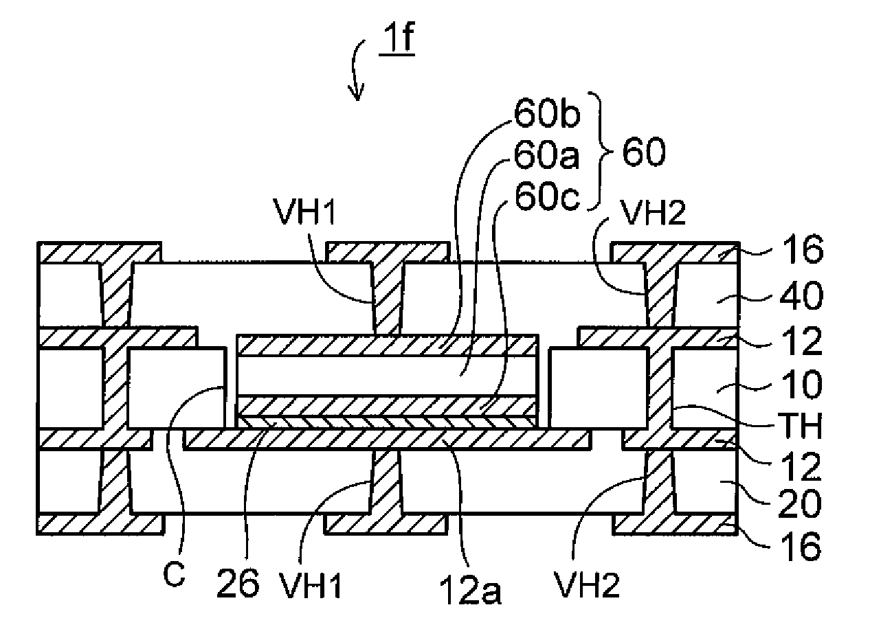
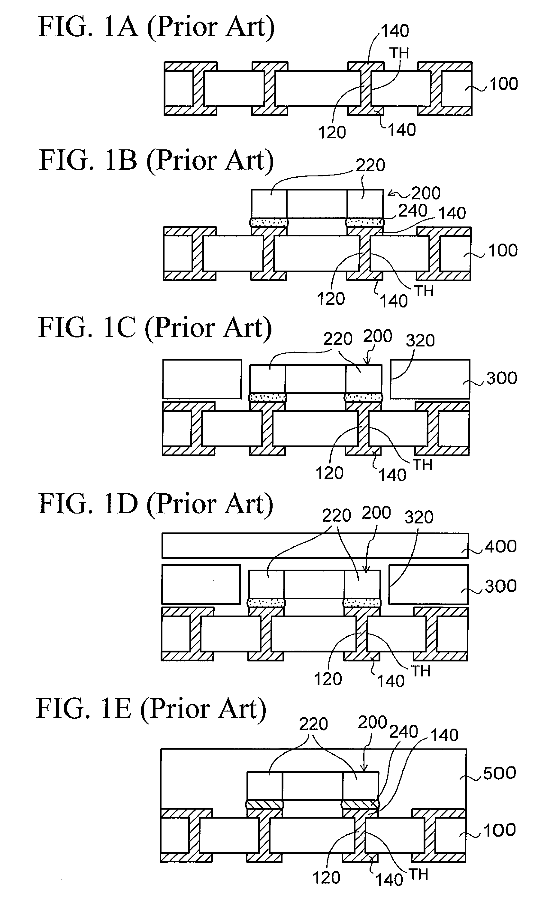
[0041]FIGS. 3A to 3D, FIGS. 4A to 4C, and FIGS. 5A to 5C are sectional views showing a method of manufacturing an electronic component built-in substrate according to a first embodiment of the present invention. In the method of manufacturing the electronic component built-in substrate according to the present embodiment, as shown in FIG. 3A, first, a core substrate 10 on both surface sides of which a first wiring layer 12 is provided respectively is prepared. The core substrate 10 is formed of an epoxy resin into which a glass cloth is contained, or the like, and through holes TH passing through the thickness direction are formed in the core substrate 10. A through electrode 14 is filled in the through holes TH of the core substrate 10 respectively, and the first wiring layers 12 on both surface sides of the core substrate 10 are connected mutually via the through electrodes 14.

[0042]Alternately, a through hole plating layer may be provided on inner surfaces of the through holes TH...

second embodiment

[0083]FIGS. 6A to 6C and FIGS. 7A and 7B are sectional views showing a method of manufacturing an electronic component built-in substrate according to a second embodiment of the present invention.

[0084]In the second embodiment, a semiconductor chip is mounted instead of the capacitor component in the first embodiment. In the second embodiment, detailed explanation about the same steps as those in the first embodiment will be omitted herein.

[0085]In the method of manufacturing the electronic component built-in substrate according to the second embodiment, as shown in FIG. 6A, first, a structure in which the stopper metal layer 12a of the bottom portion of the concave portion C of the mounted body 5 is removed is obtained, like FIG. 3C of the first embodiment.

[0086]Then, as shown in FIG. 6B, a semiconductor chip 50 (LSI chip) having connection terminals 52 (connection pads or connection bumps) is prepared. Then, the semiconductor chip 50 is mounted / bonded on the concave portion C of t...

third embodiment

[0092]FIGS. 8A to 8C are sectional views showing a method of manufacturing an electronic component built-in substrate according to a third embodiment of the present invention.

[0093]In the third embodiment, the semiconductor chip is mounted in a face-up manner in the second embodiment. In the third embodiment, detailed explanation about the same steps as those in the first embodiment will be omitted herein.

[0094]In the method of manufacturing an electronic component built-in substrate according to the third embodiment, as shown in FIG. 8A, in the above step in FIG. 6B of the second embodiment, the semiconductor chip 50 is mounted / bonded on the concave portion C of the mounted body 5 by the adhesive 34 while directing the connection terminals 52 upward (face-up).

[0095]Then, as shown in FIG. 8B, the upper interlayer insulating layer 40 is formed on the semiconductor chip 50 and the core substrate 10 by the similar method to that in the first embodiment.

[0096]Then, as shown in FIG. 8C, ...


PUM

PropertyMeasurementUnit
insulatingaaaaaaaaaa
depthaaaaaaaaaa
thicknessaaaaaaaaaa

Abstract

In a method of manufacturing an electronic component built-in substrate of the present invention, a mounted body including a first insulating layer, a stopper metal layer formed under the first insulating layer of a portion corresponding to a component mounting region and a second insulating layer formed on a lower surface of the first insulating layer and covering the stopper metal layer is prepared, and a concave portion is obtained by penetration-processing a portion of the first insulating layer, which corresponds to the component mounting region to form an opening portion, while using the stopper metal layer as a stopper. Also, the stopper metal layer in the concave portion is removed, then an electronic component is mounted on the concave portion, and then a third insulating layer is formed on the electronic component.

Description

CROSS-REFERENCE TO RELATED APPLICATIONS[0001]This application is based on and claims priority of Japanese Patent Application No. 2008-042621 filed on Feb. 25, 2008, the entire contents of which are incorporated herein by reference.BACKGROUND OF THE INVENTION[0002]1. Field of the Invention[0003]The present invention relates to a method of manufacturing an electronic component built-in substrate and, more particularly, a method of manufacturing an electronic component built-in substrate in which a passive component, a semiconductor chip, or the like is mounted to be embedded in an insulating layer.[0004]2. Description of the Related Art[0005]In the prior art, there is the electronic component built-in substrate in which the electronic component such as the capacitor, or the like is mounted to be embedded in the insulating layer. As a first method of manufacturing an electronic component built-in substrate in the prior art, as shown in FIG. 1A, first, a core substrate 100 in which a wi...

Claims


Application Information

Patent Timeline
Patent Type & Authority Applications(United States)
IPC IPC(8): H01L21/00B23K26/00B23K26/382H05K3/00H05K3/46
CPCH01L23/49822H01L23/5389H01L2224/73204H01L2224/32225H01L2224/16225H01L2924/01033H01L2924/01006H01L2924/01005H05K2203/1152H05K2201/10674H01L24/18H01L24/82H01L2224/18H01L2224/82039H01L2924/01029H01L2924/01078H01L2924/01079H01L2924/15153H01L2924/1517H01L2924/15311H01L2924/19041H01L2924/19042H01L2924/19043H05K1/0231H05K1/185H05K3/0035H05K3/06H05K3/061H05K3/4602H05K2201/09509H05K2201/10636H05K2201/10643H01L2924/00H01L24/19H01L2224/04105H01L2224/05568H01L2224/05573H01L2224/16227H01L2224/73267H01L2224/92144H01L2224/92244H01L2924/00014H01L2924/351Y02P70/50H01L2224/05599
Inventor INOUE, OSAMU
Owner SHINKO ELECTRIC IND CO LTD
Why Eureka
Try Eureka