Sample dimension inspecting/measuring method and sample dimension inspecting/measuring apparatus

a measurement method and dimension technology, applied in the direction of instruments, image enhancement, therapy, etc., can solve the problems of limited accuracy of scanning position and direction of electron beam, and the error will take place in the detection position of the pattern edge, so as to reduce the error of measurement of the pattern edge position, and improve the effect of accuracy

Active Publication Date: 2009-09-03
HITACHI HIGH-TECH CORP
View PDF11 Cites 44 Cited by
  • Summary
  • Abstract
  • Description
  • Claims
  • Application Information

AI Technical Summary

Benefits of technology

[0012]The principal advantage of the present invention is to provide sample dimension inspecting / measuring method and apparatus in which by reducing the error of measurement of a pattern edge position attributable to differences in the electron beam scanning direction and the pattern edge direction as well and by reducing the error of measurement of a pattern edge position due to errors of the scanning position and direction caused when the scanning direction of the electron beam is changed, edge positions in all directions of a fine pattern can be measured with high accuracies.

Problems solved by technology

Therefore, the Patent Document 1 and Patent Document 2 propose that the electron beam is always scanned vertically to the direction of the pattern edge of inspection objective pattern but they raise problems as below.
The accuracy of control of scanning position and direction of the electron beam is limited and in some case, when the scanning direction is changed, the pattern edge detection position will change by 1 nm or more.
Accordingly, with the electron beam managed to scan constantly vertically to the pattern edge of inspection objective pattern, an error will take place in pattern edge detection position depending on the scanning position and direction.

Method used


Image

  • Sample dimension inspecting/measuring method and sample dimension inspecting/measuring apparatus
  • Sample dimension inspecting/measuring method and sample dimension inspecting/measuring apparatus
  • Sample dimension inspecting/measuring method and sample dimension inspecting/measuring apparatus

Examples


embodiment 1

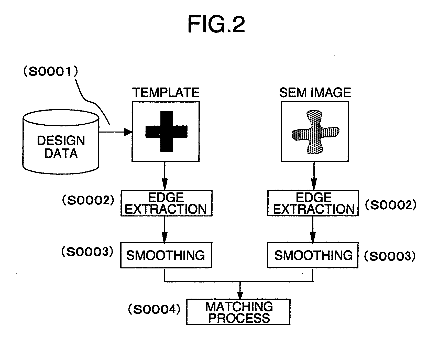
[0054]FIG. 3 illustrates a state in which an electron microscope image of an actual pattern 41 formed on a wafer (hereinafter referred sometimes to as an actual pattern) is superposed on a design pattern 40. This can be obtained by subjecting each of a binary-digitized template prepared from the design pattern 40 (S0001) and an SEM image actually acquired from the wafer to edge extraction (S0002) and smoothing (S0003) and then by subjecting them to a matching process (S0004) through the use of a normalizing function, as shown in FIG. 2.

[0055]The EPE measurement is to measure an error in shape between the ideal pattern shape indicated by the design pattern 40 and the actual pattern 41 but as will be described with reference to FIG. 3, the actual pattern 41 is often formed while being constricted at a pattern tip portion 42 and rounded at a corner portion 43, for example. In an example as shown in FIG. 3, the pattern is sorted into 1) a tip portion of pattern (hereinafter referred to ...

embodiment 2

[0062]In FIG. 7, a method of switching the scanning direction 95 of the electron beam in compliance with the EPE measurement direction. By using this method, identical signal waveforms of secondary electrons can be obtained even in respect of pattern edges in any directions. But, when the scanning direction of electron beam is changed as described previously, the scanning position will sometimes displace as shown in FIG. 8. In this example, the actual pattern 41 on SEM image when the electron beam scanning direction is 0° is indicated in solid curve, the actual pattern in the case of 180° is indicated in dotted curve and an error in the electron beam scanning direction between 0° and 180° directions is indicated by (ΔX, ΔY).

[0063]While in this example only errors in X direction and Y direction are indicated, an error in rotational direction will possibly occur. Further, there is the possibility that these errors will differ with the distance or direction of the electron beam scannin...

embodiment 3

[0064]An example of measuring a pattern edge position by using secondary electron signal waveforms obtained through scanning of (one) electron beam at one position is shown in FIG. 4 but this is disadvantageous in that the S / N ratio of signal waveform is low and the accuracy of EPE measurement is insufficient. To the contrary, a method as shown in FIG. 10 is employable according to which by using a line profile 54 created by averaging and smoothing a plurality of secondary electron signal waveforms obtained through scanning of (plural) electron beams at plural positions, the pattern edge position is measured. Since the line profile 54 has a higher S / N than every one original secondary electron signal waveform, a correct pattern edge position can be measured accurately.

[0065]By using the method as above, a correct contour of the actual pattern 41 can be detected with sub-nanometer accuracies.

[0066]The line profile can be prepared 1) by extracting pieces of information of pixels insid...


PUM

PropertyMeasurementUnit
widthaaaaaaaaaa
relative angleaaaaaaaaaa
shapeaaaaaaaaaa

Abstract

One of principal objects of the present invention is to provide a sample dimension measuring method for detecting the position of an edge of a two-dimensional pattern constantly with the same accuracy irrespective of the direction of the edge and a sample dimension measuring apparatus. According to this invention, to accomplish the above object, it is proposed to correct the change of a signal waveform of secondary electrons which depends on the direction of scanning of an electron beam relative to the direction of a pattern edge of an inspection objective pattern. It is proposed that when changing the scanning direction of the electron beam in compliance with the direction of a pattern to be measured, errors in the scanning direction and the scanning position are corrected. In this configuration, a sufficient accuracy of edge detection can be obtained irrespective of the scanning direction of the electron beam.

Description

TECHNICAL FIELD[0001]The present invention relates to a pattern inspecting / measuring method, a pattern inspecting / measuring apparatus and a computer program for performing inspection / critical dimension of a pattern and more particularly, to a method and apparatus for inspecting / measuring the shape or placement error concerning a pattern by comparing design data of the pattern with an actual pattern.BACKGROUND ART[0002]It has been known to measure a circuit pattern of semiconductor device actually formed on a wafer by using a design data of the circuit pattern of semiconductor device. Since the design of the circuit pattern shows an ideal shape the circuit pattern of semiconductor device has primarily, the accuracy of patterning by a semiconductor fabrication process can be evaluated by comparing the design data with a pattern actually formed on the wafer.[0003]Recently, fineness of a semiconductor integrated circuit has been advancing and in the wake thereof, the performance of a se...

Claims


Application Information

Patent Timeline
Patent Type & Authority Applications(United States)
IPC IPC(8): G01N23/00
CPCG01B15/04G03F1/0092G03F1/86G06T7/001G06T7/0085H01J2237/2817G06T2207/30148H01J37/222H01J37/28H01J2237/24592G06T2207/10061G06T7/13
Inventor MOROKUMA, HIDETOSHISUGIYAMA, AKIYUKIMATSUOKA, RYOICHISUTANI, TAKUMICHITOYODA, YASUTAKA
Owner HITACHI HIGH-TECH CORP
Why Eureka
Try Eureka