Highly Conductive Shallow Junction Formation

a technology of shallow junctions and high conductive conductivity, which is applied in the direction of semiconductor devices, electrical equipment, transistors, etc., can solve the problems of increasing reverse bias leakage, affecting the effect of reverse bias, and reducing the diffusion rate of the devi

Inactive Publication Date: 2009-09-10
TEXAS INSTR INC
View PDF11 Cites 96 Cited by
  • Summary
  • Abstract
  • Description
  • Claims
  • Application Information

AI Technical Summary

Problems solved by technology

The formation of ultra-shallow junctions, that is, junctions having source / drain regions no more than about 35 nm thick and with a dopant concentration not less than 5×10¹⁹ atoms / cm3, is considered one of the significant challenges in manufacturing the next generation of CMOS devices.
Such conventional anneal processes result in a modest amount of diffusion.
While SPER of amorphous doped regions is effective in forming shallow implants with high dopant concentrations, there are obstacles to its implementation.
These defects, which are thought to involve interstitial silicon atoms, increase reverse bias leakage (and thereby increase Off-State current).
Thus, there remains an unsatisfied need for effective methods of forming ultra-shallow junctions.

Method used


Image

  • Highly Conductive Shallow Junction Formation
  • Highly Conductive Shallow Junction Formation
  • Highly Conductive Shallow Junction Formation

Examples


Embodiment Construction

[0019]The present invention will now be described with reference to the attached drawings, wherein like reference numerals are used to refer to like elements throughout. Exemplary processes comprising series of acts and events are provided. The present invention is not limited by the ordering of the acts and events in these examples as some acts may occur in different orders and / or concurrently with other acts or events. In addition, not all illustrated acts or events are required to implement a methodology in accordance with the present invention.

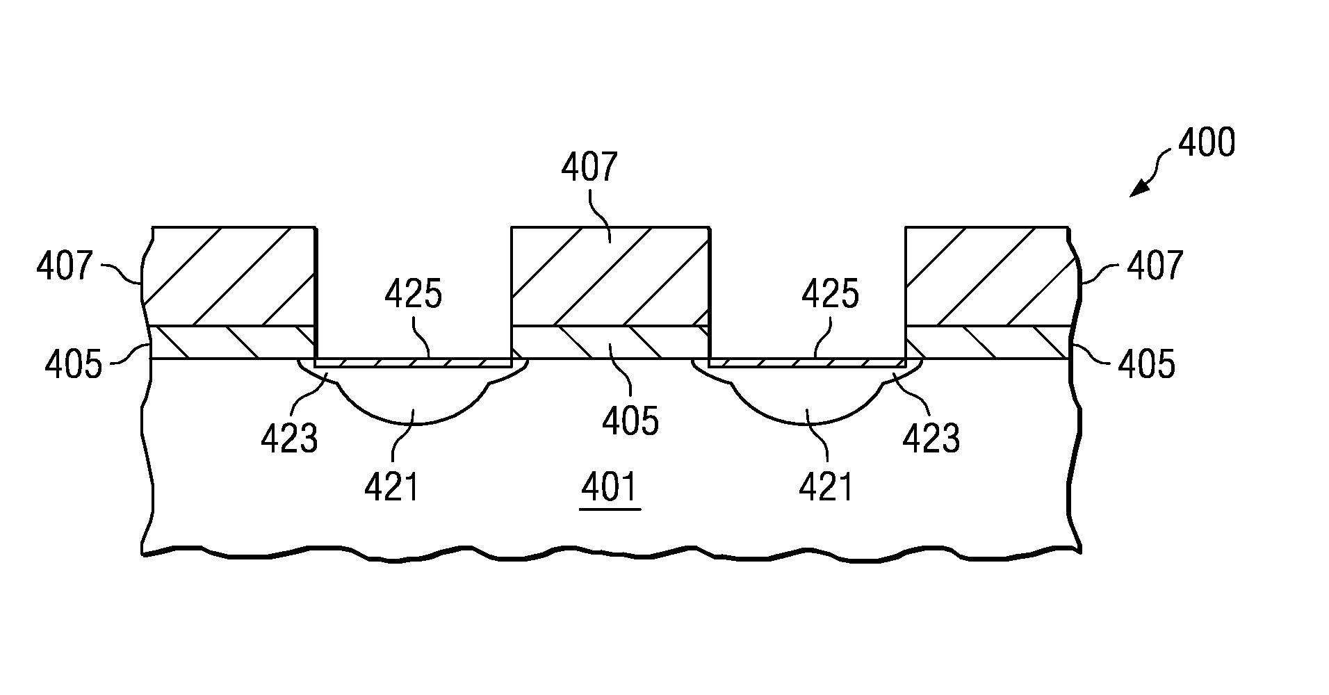
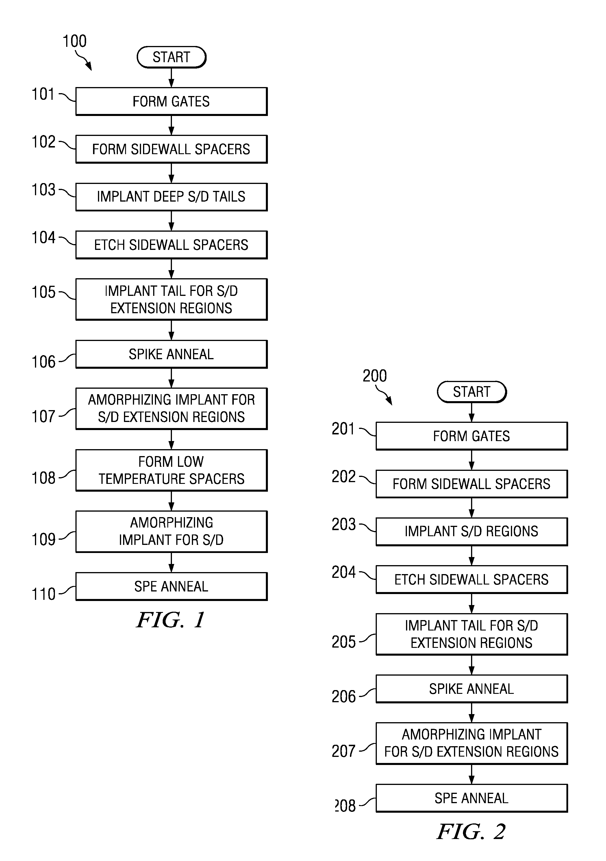
[0020]FIG. 1 illustrates an exemplary process 100 for forming a P-N junction within a semiconductor substrate according to one aspect of the present invention. The process 100 includes gate formation 101, forming sidewall spacers 102, forming deep source / drain implants 103, and etching away the sidewall spacer 104. The process further includes forming a source / drain extension region tail implant 105, annealing to activate the dopants 106, ...


PUM


Abstract

The invention relates to a method of forming a shallow junction. The method (100) comprises forming source / drain extension regions with a non-amorphizing tail implant (105) which is annealed conventionally (spike / RTP) and amorphizing implant which is re-grown epitaxially(SPER) (110). The non-amorphizing tail implant is generally annealed (106) before a doped amorphous layer for SPE is formed (107). SPE provides a high active dopant concentration in a shallow layer. The non-amorphizing tail implant (105) expands the source / drain extension region beyond the range dictated by the SPE-formed layer and keeps the depletion region of the P-N junction away from where end-of-range defects form during the SPE process. Thus, the SPE-formed layer primarily determines the conductivity of the junction while the tail implant determines the location of the depletion region. End-of-range defects form, but are not in a position to cause significant reverse bias leakage.

Description

FIELD OF THE INVENTION[0001]The present invention relates generally to semiconductor device manufacturing and more particularly to methods of manufacturing devices with ultra-shallow junctions.BACKGROUND OF THE INVENTION[0002]In the semiconductor industry, there is a continuing trend toward high device densities. To achieve these high device densities, small features on semiconductor wafers are required. These features include source regions, drain regions, and channel regions that relate to devices, such as field effect transistors (FETs).[0003]In the process of scaling down complementary metal oxide semiconductor (CMOS) devices, which are a type of FET, a vertical dimension must be reduced at the same time as horizontal dimensions are reduced. In particular, in order to avoid short channel effects, source and drain regions, or at least source / drain extension regions adjacent the channel, must be made extremely shallow with a corresponding increase in dopant density to avoid excess...

Claims


Application Information

Patent Timeline
Patent Type & Authority Applications(United States)
IPC IPC(8): H01L29/78
CPCH01L21/26506H01L21/324H01L29/7833H01L29/6653H01L29/6659H01L21/823814H01L21/26513
Inventor KOHLI, PUNEET
Owner TEXAS INSTR INC
Why Eureka
Try Eureka