Imprint method and template for imprinting

a technology of imprinting and printing method, which is applied in the direction of electric/magnetic/electromagnetic heating, instruments, photomechanical equipment, etc., can solve the problems of difficult to achieve resolution to the extent that complies with the latest design rule, and become difficult to form a miniaturized pattern

Active Publication Date: 2009-09-10
KIOXIA CORP
View PDF11 Cites 40 Cited by
  • Summary
  • Abstract
  • Description
  • Claims
  • Application Information

AI Technical Summary

Benefits of technology

[0011]A template for imprinting according to an embodiment of the present invention comprises: a pattern formed region including a concave-convex pattern for element pattern printing; and a pattern periphery region existing in a periphery of the pattern formed region, a transmittance of the pattern periphery region being less than a transmittance of a concave pattern in the concave-convex pattern.

Problems solved by technology

In recent years, along with a progress of down-sizing of a semiconductor device, problems that may occur in a photolithography process used in the manufacturing process of the semiconductor device have become more apparent.
However, with a conventional lithography technique where a miniaturized pattern is exposed to light, it is difficult to achieve resolution to the extent that complies with the latest design rule.
Consequently, it has become difficult to form a miniaturized pattern to such an extent that meets the latest design rule.
However, when a comparatively thick hardened organic material portion in the pattern printed region (also referred to as a shot) where the pattern has already been formed by the organic material being hardened extends into an adjacent shot as being a patterning target, downward movement of the template as performed in patterning of the adjacent shot lying next to the target shot may be interfered with the hardened organic material.
When the downward movement of the template is interfered, the template and the organic material will not be able to contact sufficiently with each other in the pattern printing region as being a patterning target.
As a result, printing deficiency may occur.
Therefore, the whole substrate surface cannot be used effectively for pattern formation, and the number of shots which can be formed on the substrate is to be limited.

Method used


Image

  • Imprint method and template for imprinting
  • Imprint method and template for imprinting
  • Imprint method and template for imprinting

Examples


first embodiment

[0046]A first embodiment of the present invention will be described. According to the first embodiment, exposing time for a region corresponding to a pattern periphery region of a substrate is adjusted, for instance, by shutting out light by a shutter (which is a light shielding member) for a predetermined period of time.

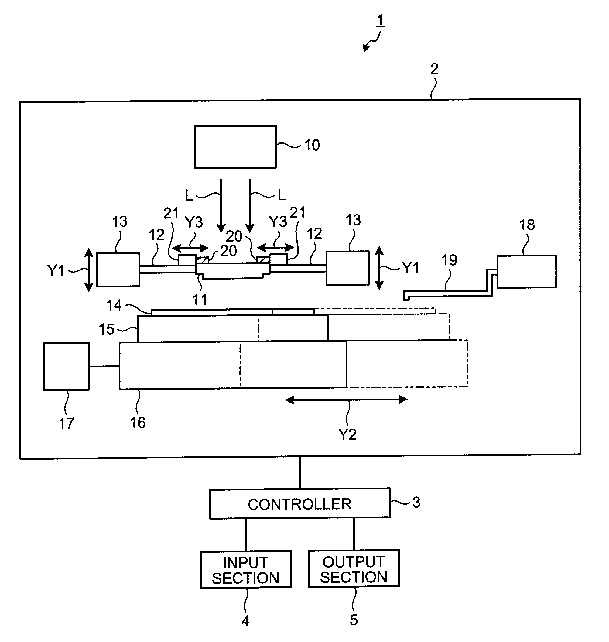
[0047]FIG. 1 is a schematic view showing one example of a structure of a nano-imprint apparatus according to the first embodiment of the present invention. As shown in FIG. 1, the nano-imprint apparatus 1 according to the first embodiment includes a nano-imprint machine 2, a controller 3, an input section 4, and an output section 5. The nano-imprint machine 2 executes pattern printing on a substrate 14 using the nano-imprint technique, the substrate 14 being a sample. The controller 3 controls an operation of each of the constructing parts of the nano-imprint apparatus 1. The input section 4 inputs instruction regarding processing operation of the nano-imprint appar...

second embodiment

[0079]A second embodiment of the present invention will be described. In the second embodiment, for example, a transmissive film with a predetermined transmittance is arranged between the substrate and the light source, for the purpose of adjusting light intensity in exposure with respect to the region on the surface of the substrate corresponding to the pattern periphery region.

[0080]FIG. 12 is a schematic diagram showing one example of a structure of a nano-imprint apparatus according to the second embodiment. As shown in FIG. 12, a nano-imprint apparatus 201 according to the second embodiment has a nano-imprint machine 202 which does not have the shutter (corresponding to the shutter 20 shown in FIG. 1) or the shutter moving units (corresponding to the shutter moving unit 21 shown in FIG. 1). Meanwhile, instead of the template 11 as shown in FIG. 1, the nano-imprint machine 202 has a template 211 where a transmissive film 220 with a predetermined transmittance is arranged. Moreov...


PUM

PropertyMeasurementUnit
sizeaaaaaaaaaa
exposing timeaaaaaaaaaa
light intensityaaaaaaaaaa

Abstract

An imprint method, in which pattern forming is performed by having a light curable material applied on a sample face of a substrate being a processing target hardened by being exposed to light in a state where the light curable material and a pattern formed surface of a template contact each other, the pattern formed surface having a concave-convex pattern formed thereon; wherein in one exposure performed with respect to a predetermined shot of the light curable material, an exposure amount at a light curable material on a first region which contacts a pattern formed region including the concave-convex pattern of the template is greater than an exposure amount at a light curable material on a second region which at least contacts a part of a pattern periphery region of the template, the pattern periphery region existing in a periphery of the pattern formed region of the template.

Description

CROSS-REFERENCE TO RELATED APPLICATIONS[0001]This application is based upon and claims the benefit of priority from the prior Japanese Patent Application No. 2008-56394, filed on Mar. 6, 2008; the entire contents of which are incorporated herein by reference.BACKGROUND OF THE INVENTION[0002]1. Field of the Invention[0003]The present invention relates to an imprint method for pattern forming in a semiconductor manufacturing process, and to a template for imprinting.[0004]2. Description of the Related Art[0005]In recent years, along with a progress of down-sizing of a semiconductor device, problems that may occur in a photolithography process used in the manufacturing process of the semiconductor device have become more apparent. That is, in the recent leading-edge rules for designing a semiconductor device based on half-pitch, a pitch size has been reduced down to 22 nm. However, with a conventional lithography technique where a miniaturized pattern is exposed to light, it is difficu...

Claims


Application Information

Patent Timeline
Patent Type & Authority Applications(United States)
IPC IPC(8): B29C59/16G03F7/00B81C99/00
CPCB82Y10/00G03F7/0002B82Y40/00
Inventor MIKAMI, SHINJIYONEDA, IKUO
Owner KIOXIA CORP
Why Eureka
Try Eureka