
Semiconductor integrated circuit device and method for evaluating an eye-opening margin

a technology of integrated circuit and eye opening margin, which is applied in the direction of digital transmission, pulse automatic control, instruments, etc., can solve the problems of inability to accurately the inability to measure the eye opening margin by a simple accompanying clock system, and achieve the effect of high accuracy

Inactive Publication Date: 2009-09-10
HITACHI LTD
View PDF15 Cites 21 Cited by
  • Summary
  • Abstract
  • Description
  • Claims
  • Application Information

AI Technical Summary

Benefits of technology

[0013]The invention makes it possible to make eye-opening margin measurement with high accuracy in a high-speed serial data reception circuit. Particularly, it is possible to measure the eye-opening margin of received data including a jitter component of a clock data recovery circuit of a data lane. Also, in the measurement circuit, an error acceleration test can be conducted by applying an offset pulse from the pulse-forming circuit to add any jitter component.

Problems solved by technology

However, because a clock signal itself has a jitter component, it is impossible to measure the eye-opening margin accurately.
Besides, in Gbps-order transmissions, considering lane-to-lane skews of high-speed serial data or distribution skews of accompanying clocks, eye-opening margin cannot be measured accurately by a simple accompanying clock system.

Method used


Image

  • Semiconductor integrated circuit device and method for evaluating an eye-opening margin
  • Semiconductor integrated circuit device and method for evaluating an eye-opening margin
  • Semiconductor integrated circuit device and method for evaluating an eye-opening margin

Examples


Embodiment Construction

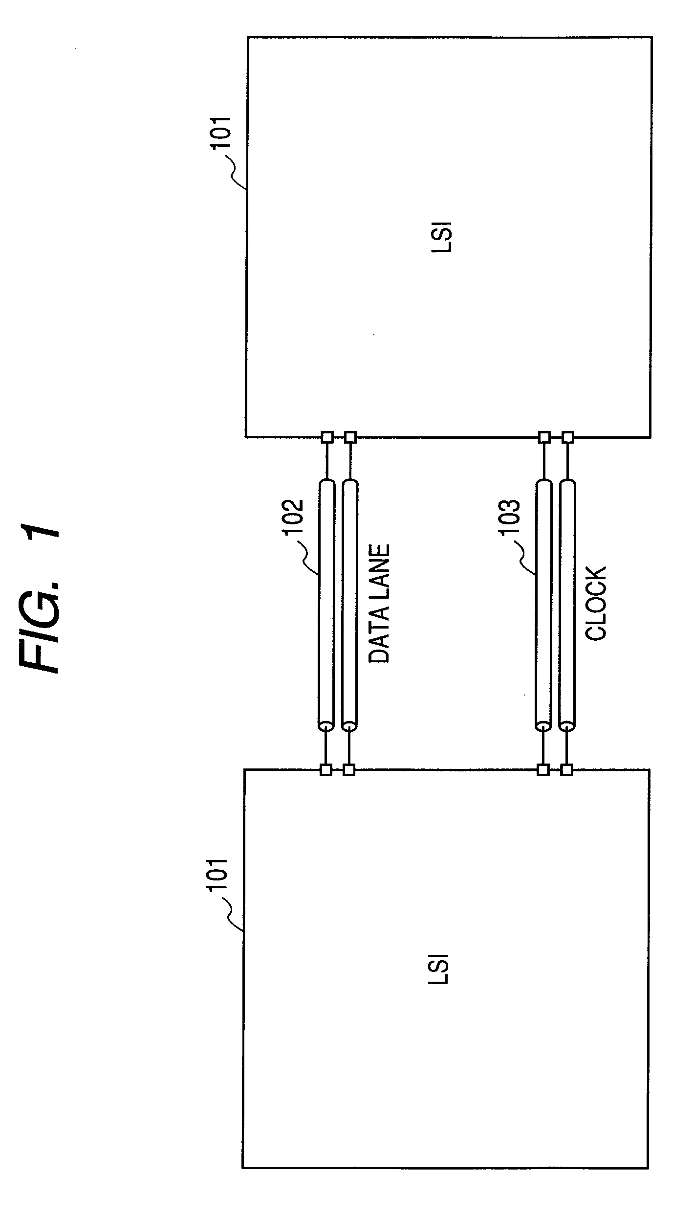
[0024]Next, the preferred embodiment of the present invention will be described in detail. FIG. 1 shows a high-speed serial data transmission system configuration according to the embodiment of the present invention. The high-speed serial data transmission / reception system includes LSIs 101 and a transmission system comprised of data lanes 102 and accompanying clock lanes 103.

[0025]The LSIs 101 are semiconductor devices capable of transmitting and receiving serial data at high speed. The data lanes 102 transmit high-speed serial data generated between the LSIs 101. The accompanying clock lanes 103 transmit clock signals having phase information representative of all data lanes.

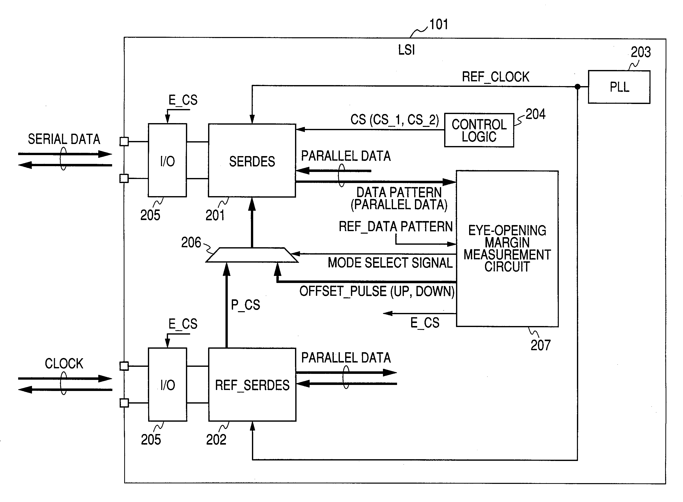
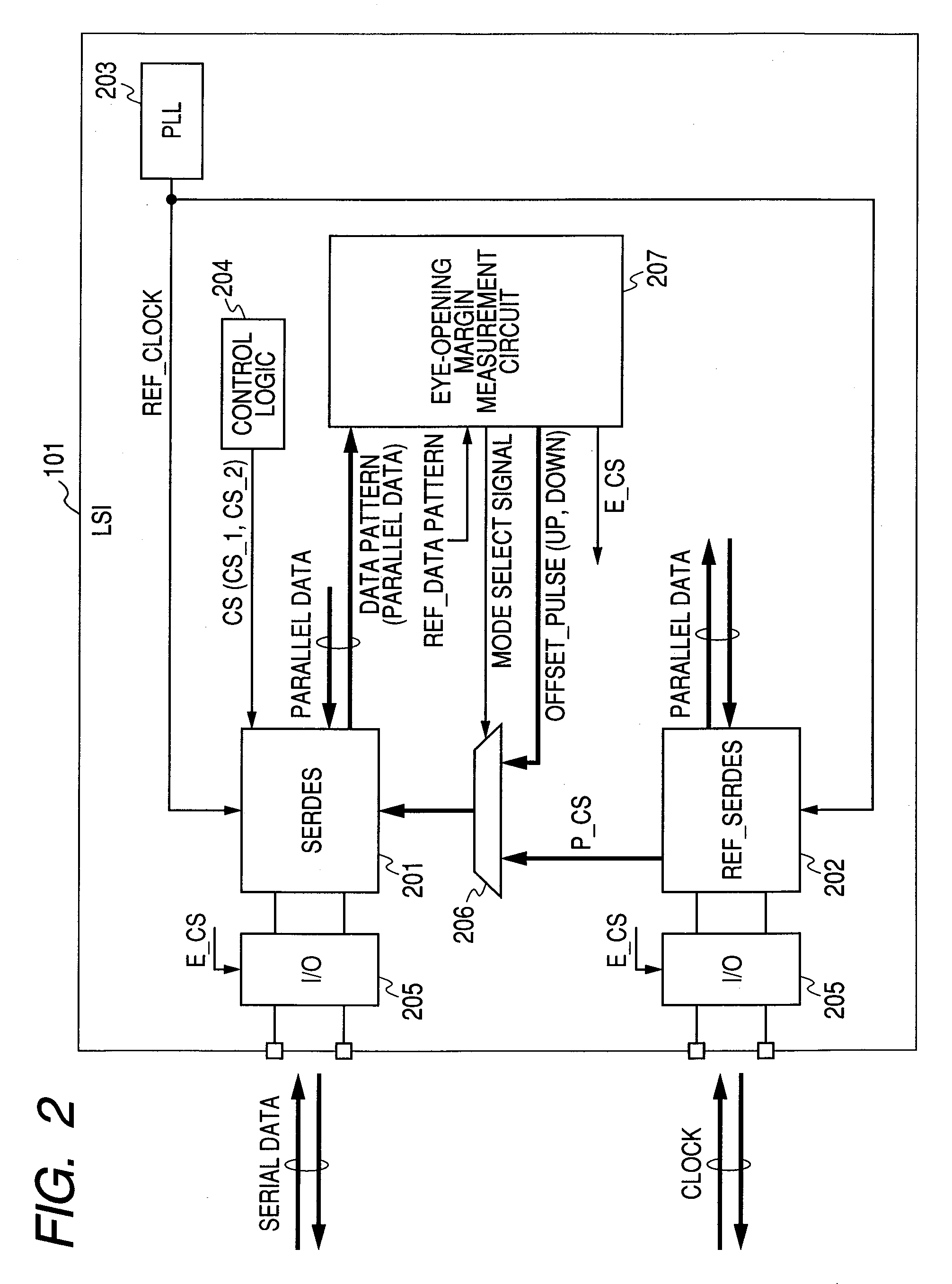
[0026]FIG. 2 shows details of an LSI 101 in FIG. 1. It is comprised of: an accompanying clock high-speed serial data transmission system which includes multiple SerDes circuits 201, a Ref_SerDes circuit 202, a Phase Locked Loop circuit 203 (PLL), a control logic circuit 204 (Control Logic) and I / O circuits 205...


PUM


Abstract

An eye-opening margin measurement method for a high-speed serial data reception circuit which uses a circuit for eye-opening margin measurement involving operation of a clock data recovery circuit without fixing the clock phase. In this method, an error acceleration test can also be made on received data by giving an offset pulse signal to phase information to add a jitter component. The method uses a semiconductor integrated circuit device which includes a serializer / deserializer circuit (SerDes) for receiving serial data and a reference serializer / deserializer circuit (Ref_SerDes) for receiving an accompanying clock signal. The SerDes circuit converts received serial data into parallel data through a recovery clock whose phase is controlled using phase control signal P_CS generated by the Ref_SerDes circuit. An offset pulse signal Offset_Pulse from the pulse-forming circuit is applied to the phase control signal P_CS to make eye-opening margin measurement.

Description

CLAIM OF PRIORITY[0001]The present application claims priority from Japanese patent application JP 2008-055696 filed on Mar. 6, 2008, the content of which is hereby incorporated by reference into this application.FIELD OF THE INVENTION[0002]The present invention relates to a semiconductor device and more particularly to a technique which measures an eye-opening margin as an index for received data signal waveform quality for use in high speed data transmission between devices.BACKGROUND OF THE INVENTION[0003]In recent years, serial data transmissions have been the mainstream in high speed data transmissions between devices. In a high speed serial data transmission between semiconductor devices, a serializer / deserializer (SerDes) is used to convert outgoing parallel data into serial data and convert incoming serial data into parallel data. Since attenuation in transmission lines is more serious at higher transmission speed, it is important to evaluate the waveform quality in the rece...

Claims


Application Information

Patent Timeline
Patent Type & Authority Applications(United States)
IPC IPC(8): H03L7/00
CPCH03L7/08H04L1/205H04L7/043H04L7/0331H04L7/0008
Inventor MATSUMOTO, AKIRAHAMANO, DAISUKEHAYASHI, ATSUHIROSUZUKI, KZUHISA
Owner HITACHI LTD
Learn More