

Reticle for projection exposure apparatus and exposure method using the same
- Summary
- Abstract
- Description
- Claims
- Application Information
AI Technical Summary
Benefits of technology
Problems solved by technology
Method used
Image

Examples
first embodiment
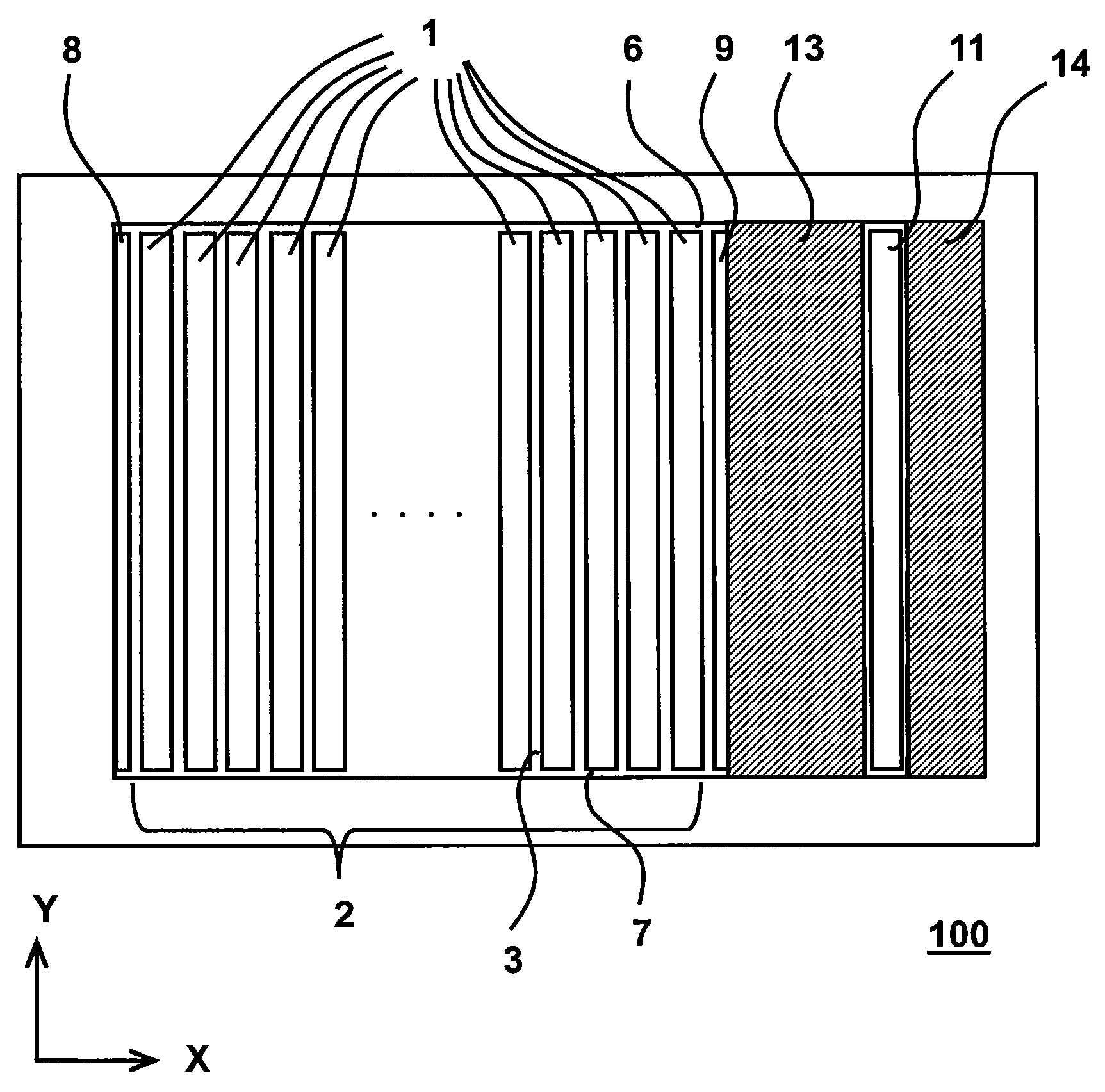
[0022]FIG. 1 is a plan view of a reticle for a projection exposure apparatus according to the present invention. A reticle substrate 100 is formed of a transparent low-expansion material such as synthetic quartz, and a pattern is formed on one surface thereof by using a light-shielding film of, for example, chromium oxide. Ordinarily, the surface of the reticle substrate 100 to which a chromium oxide film is attached is covered with a pellicle film, which is omitted in FIG. 1, for protection when used.
[0023]Ordinarily, in a projection exposure method, a size of the pattern on the reticle is different from a size of a pattern transferred onto a wafer. A magnification of ⅕ reduction is often used. The magnification means that, if the size of the pattern on the reticle is 100 μm, for example, the size of the pattern transferred onto the wafer is reduced to 20 μm. In the following description, all dimensions are dimensions of the pattern transferred onto the wafer.
[0024]N chip regions 1...
second embodiment
[0038]FIG. 3 is a plan view of a reticle for a projection exposure apparatus according to the present invention.
[0039]The reticle illustrated in FIG. 3 is different from that illustrated in FIG. 1 in that a left end scribe line region 4 is arranged on the left of the first alignment mark arrangement region 8 while a right end scribe line region 5 is arranged on the right of the second alignment mark arrangement region 9 so that the sum of the length of the first alignment mark arrangement region 8 in the second direction, the length of the second alignment mark arrangement region 9 in the second direction, and the length of the scribe line region in the second direction (width of the scribe line) is the same as the length of the chip region 1 in the second direction. It is to be noted that, the length of the first alignment mark arrangement region 8 in the second direction may be different from the length of the second alignment mark arrangement region 9 in the second direction, but...
third embodiment
[0044]FIG. 4 is a plan view of a reticle for a projection exposure apparatus according to the present invention.
[0045]The reticle illustrated in FIG. 4 is different from that illustrated in FIG. 1 in that two chip regions are arranged in the first direction. The first alignment mark arrangement region 8 is vertically divided into two, the second alignment mark arrangement region 9 is vertically divided into two, and, similarly, the TEG pattern region 11 is vertically divided into two. The scribe line region 3 is formed also between the regions vertically divided into two. This eliminates a silicon oxide film, a silicon nitride film, a metal film, or the like which is an obstacle to separating the chips from one another in portions along which the chips are separated from one another, and thus, smooth chip separation is made possible. More specifically, cracks in the chips and peeling off of a film when the chips are separated from one another can be prevented, the number of chips pe...
PUM
 Abstract
Description
Claims
Application Information