Organic electroluminescent device, display and illuminating device

a technology of electroluminescent devices and illuminating devices, which is applied in the direction of discharge tubes/lamp details, discharge tubes luminescnet screens, other domestic articles, etc., can solve the problems of insufficient efficiency and lifetime, insufficient efficiency of light-emitting devices employing fluorescent dopants as light-emitting materials, and insufficient efficiency of light-emitting devices employing phosphorescent dopants. achieve high emission efficiency, high emission luminance, and high emission efficiency

Inactive Publication Date: 2009-09-24
MERCK PATENT GMBH
View PDF4 Cites 40 Cited by
  • Summary
  • Abstract
  • Description
  • Claims
  • Application Information

AI Technical Summary

Benefits of technology

[0038]The present invention can provide an organic EL device having high emission luminance and high emission efficiency, and particularly a blue-light emitting organic EL dev...

Problems solved by technology

Further, a sufficient emission efficiency is not attained in another color emission, particularly in blue light emission, where there is room to be improved.
However, a blue light-emitting device e...

Method used


Image

  • Organic electroluminescent device, display and illuminating device
  • Organic electroluminescent device, display and illuminating device
  • Organic electroluminescent device, display and illuminating device

Examples


example 1

Preparation of organic EL device Samples 1-1

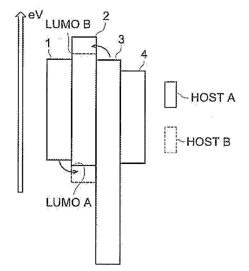
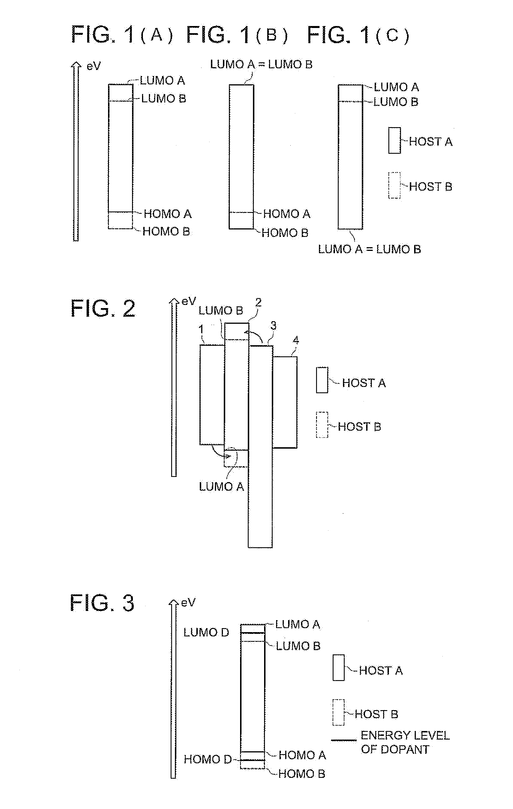
[0183]A pattern was formed on a substrate (NA45, manufactured by NH Technoglass Co., Ltd.) composed of a glass plate (100 mm×100 mm×1.1 mm) and a 100 nm ITO (indium tin oxide) layer as an anode. Then the resulting transparent substrate having the ITO transparent electrode was subjected to ultrasonic washing in isopropyl alcohol and dried by a dry nitrogen gas and subjected to UV-ozone cleaning for 5 minutes. The thus obtained transparent substrate was fixed on a substrate holder of a vacuum deposition apparatus available on the market. Further, 200 mg of m-MTDATXA were put in a first resistive heating molybdenum boat, 200 mg of Compound 1 were put in a second resistive heating molybdenum boat, 200 mg of Compound 2 were put in a third resistive heating molybdenum boat, 100 mg of PL-26 were put in a fourth resistive heating molybdenum boat, 100 mg of Compound 3 were put in a fifth resistive heating molybdenum boat, and 200 mg of Alq3 were pu...

example 2

Inventive: Preparation and Evaluation of Organic EL Device sample 3-1

[0200]A 55 nm thick hole transporting layer 3, a 30 nm light emission layer 4, a 10 nm thick hole inhibiting layer comprised of BAlq, a 40 nm thick electron transporting layer 5 comprised of Alq3, a 0.5 nm cathode buffer layer 6 comprised of lithium fluoride and a 100 nm cathode 7 comprised of Aluminum were provided on that order on the glass substrate 1 with an ITO transparent anode in a similar manner as Example 1. The hole transporting layer 3 was comprised of a 40 nm first hole transporting layer of m-MTDATA and a 15 nm second hole transporting layer of m-MTDATAX provided in that order. The light emission layer 4 was comprised of three layers, i.e., a 15 nm first layer doped with a blue phosphorescence-emitting phosphorescent compound PL-26 in an amount of 3% based on the total amount of Compounds 1 and 2, a 5 nm second layer of Compound 5 and a 10 nm third layer doped with a red phosphorescence-emitting phosph...

example 3

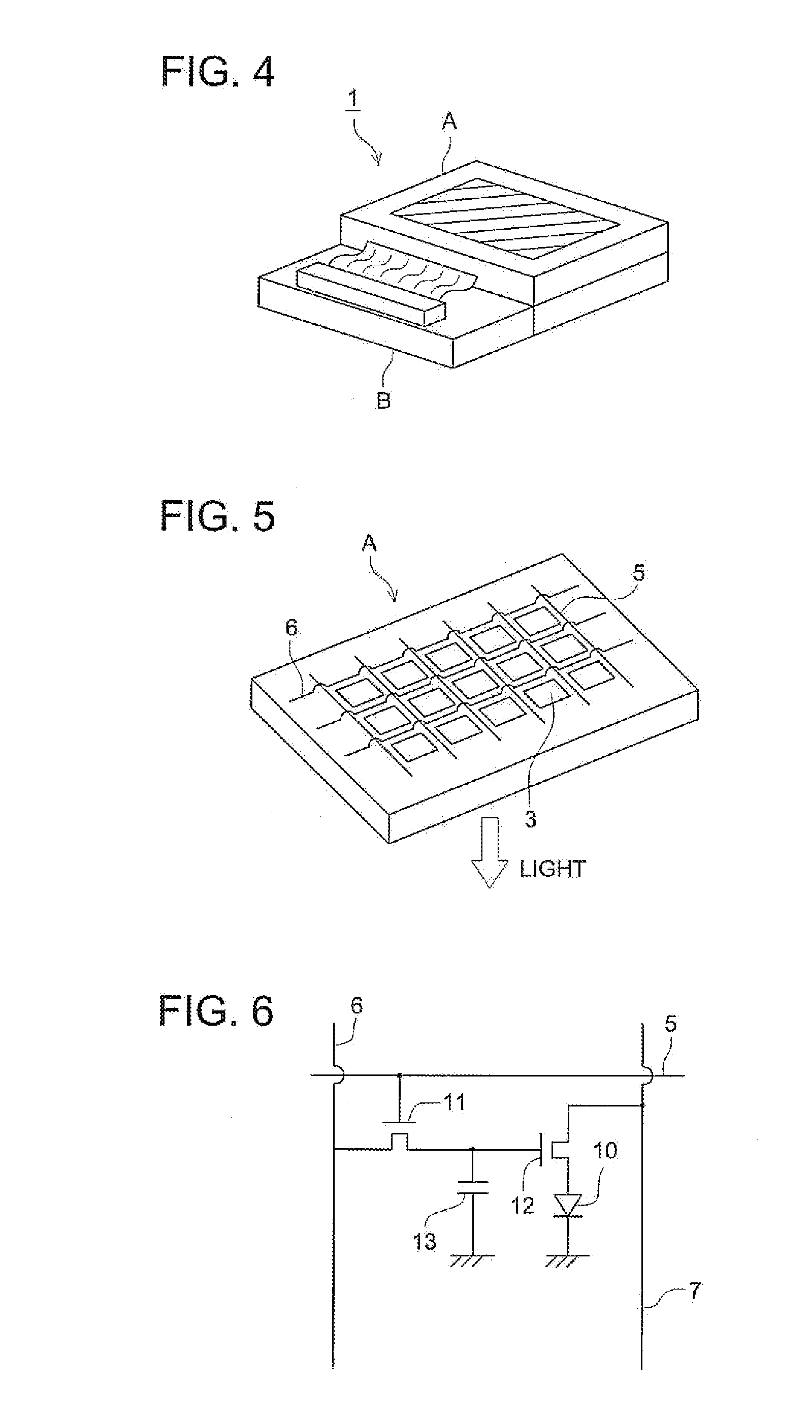
[0203]The non-emitting surface of organic EL device sample 3-1 obtained above was covered with a glass plate to obtain an illuminating device. The illuminating device can be used as a thin, white light-emitting illuminating device with high emission efficiency, high power efficiency and long emission lifetime. FIG. 9 is a schematic drawing of an illuminating device. FIG. 10 is a sectional view of an illuminating device.


PUM


Abstract

Disclosed is an organic electroluminescent (EL) device having high emission luminance and high emission efficiency. Particularly disclosed are a blue-light emitting organic EL device, which is high in emission luminance, color purity, emission efficiency and durability, a display and an illuminating device each employing the organic EL device. The organic El device is characterized in that it comprises a light emission layer containing two or more kinds of host compounds and at least one dopant, wherein at least one of the two or more kinds of host compounds has an excited triplet energy of not less than 2.7 eV, and the dopant is a phosphorescent compound.

Description

FIELD OF THE INVENTION[0001]This invention relates to an organic electroluminescent device (hereinafter also referred to as an EL device), and a display and an illuminating device each employing the same, and particularly to an EL device emitting light with high emission efficiency, and a display and an illuminating device each employing the same.TECHNICAL BACKGROUND[0002]As an emission type electronic displaying device, there is an electroluminescent device (ELD). As elements constituting the ELD, there are an inorganic electroluminescent device and an organic electroluminescent device. The inorganic electroluminescent device has been used for a plane-shaped light source, but a high voltage alternating current has been required to drive the device.[0003]An organic EL device has a structure in which a light emission layer containing a light emission compound is arranged between a cathode and an anode, and an electron and a hole were injected into the light emission layer and recombi...

Claims


Application Information

Patent Timeline
IPC IPC(8): H01J1/62
CPCC09K11/025C09K2211/1007C09K2211/1011C09K2211/1014C09K2211/1029C09K2211/1033C09K2211/1037C09K2211/104C09K2211/1044C09K2211/1048C09K2211/1051C09K2211/1055C09K2211/1059C09K2211/107C09K2211/1074C09K2211/1088C09K2211/1092C09K2211/185H05B33/14H05B33/20Y10S428/917C09K11/06H10K85/324H10K85/342H10K85/6572H10K50/125H10K50/11H10K2101/10H10K2101/30
Inventor TAMARU, JUNKOKITA, HIROSHIKATOH, EISAKUYASUKAWA, NORIKO
Owner MERCK PATENT GMBH
Why Eureka
Try Eureka