Probe card substrate with bonded via

a technology of bonded via and probe card, which is applied in the direction of electrical testing, measurement devices, instruments, etc., can solve the problems of increasing the time required to manufacture a finished probe card assembly, ltcc/htcc substrates are not ideal substrates for mems manufacturing, and the time required to manufacture space transformers and probe contactors is typically the most time-consuming. , to achieve the effect of significant time saving

Active Publication Date: 2009-09-24
FORMFACTOR INC
View PDF4 Cites 52 Cited by
  • Summary
  • Abstract
  • Description
  • Claims
  • Application Information

AI Technical Summary

Benefits of technology

[0007]Embodiments of the present invention are directed to a probe card assembly utilizing a single probe contactor substrate, or a plurality of probe contactor substrates, having a plurality of openings (holes 1100, or in many cases slots, including vertical slots 1110 and horizontal slots 1120) cut entirely through the probe contactor substrate and that run longitudinally / laterally and that vary in size and shape as shown in FIG. 11. The individual probe contactors are connected to terminals using wire bonds (the terminals are usually gold pads but other structures are commonly known in the art of wire bonding) on the space transformer through the slots in the probe contactor substrate. Because the probe contactor substrate and space transformer are separate substrates, the space transformer can be manufactured at the same time the probe head (the probe contactor substrate with the contactors attached) is being manufactured. A manufacturing timeline for such a process is shown in FIG. 13, and when compared to the traditional manufacturing process shown in FIG. 12, significant time savings are realized. Additionally, because the probe contactor substrate is not the space transformer and thus, does not need to be punched, printed, and co-fired as in the prior art, the probe contactor substrate and space transformer may be formed of different materials having more desirable qualities for their respective functions.

Problems solved by technology

If chips are found to be defective, they may be discarded when the chips are diced from the wafer, and only the reliable chips are packaged.
However, this serial approach greatly increases the time required to manufacture a finished probe card assembly.
Manufacturing the space transformer and the probe contactors are typically the most time consuming steps which is several weeks.
However, LTCC / HTCC substrates are not the ideal substrates for MEMS manufacturing.
They neither offer the optimum surface quality nor the optimum strength required for forming MEMS probe contactors on a substrate.
All of these steps add complexity and time to the fabrication process.
Additionally, substrates other than LTCC / HTCC are better suited for via redistribution, the primary function of the space transformer, however they lack the strength, thermal properties, or compatibility for MEMS manufacturing.

Method used


Image

  • Probe card substrate with bonded via
  • Probe card substrate with bonded via
  • Probe card substrate with bonded via

Examples


Embodiment Construction

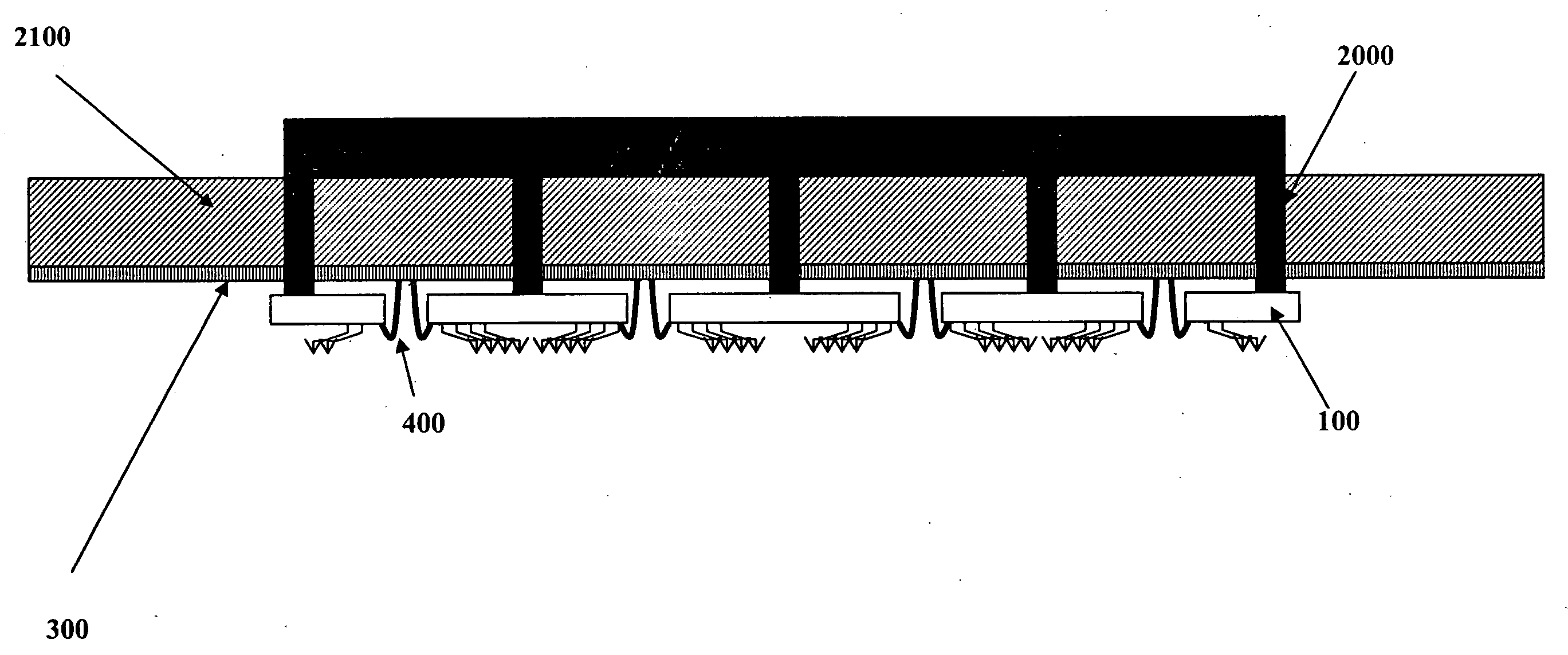
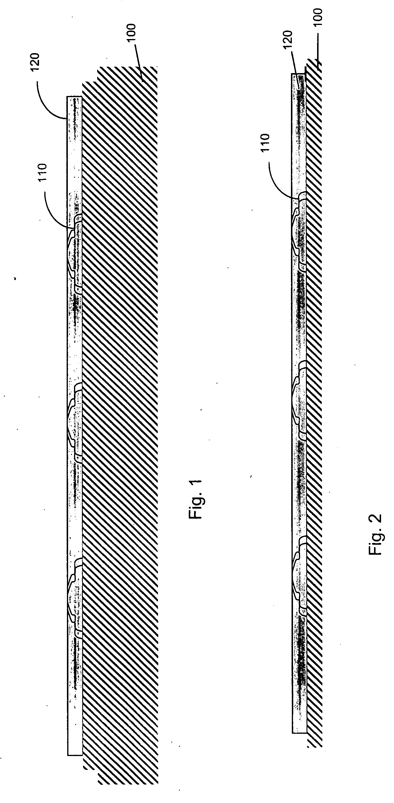
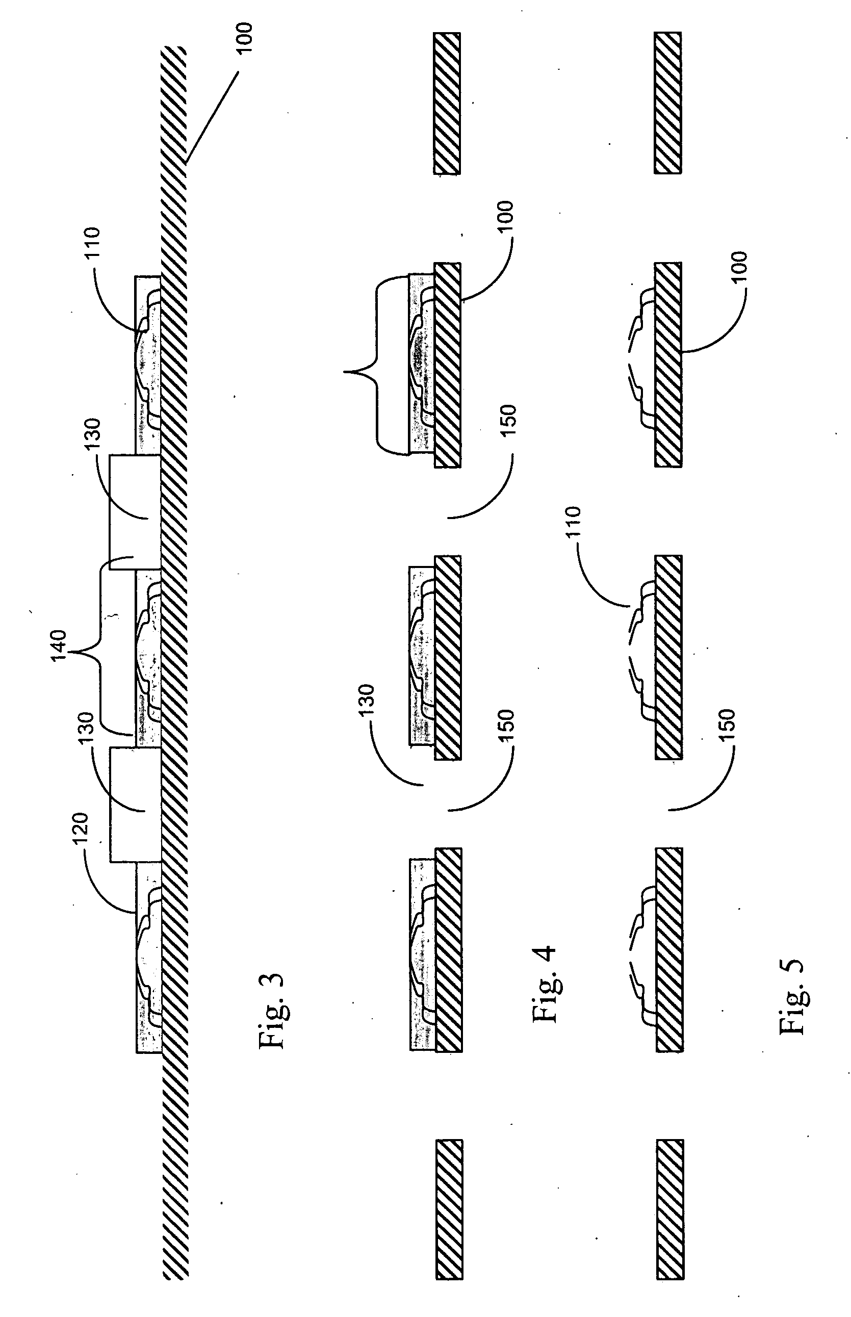
[0023]FIGS. 1-8 illustrate a process for forming an embodiment of the present invention. As shown in FIG. 1, a probe contactor substrate 100 is chosen. Because of the unique way in which the probe card assembly is fashioned, the probe contactor substrate 100 is not limited to materials generally used as probe contactor substrates, namely LTCC, HTCC, ceramics with vias, or multi-layer HDI substrates. Because the probe contactor substrate does not require electrical vias through the substrate, the substrate may be any suitable material. In an embodiment of the present invention the probe contactor substrate 100 is an alumina ceramic substrate. When used to test semiconductors, generally the probe contactor substrate should exhibit qualities such as good thermal expansion matching that of silicon (because the device under test is usually silicon), good surface quality (low pitting, excellent planarity and surface roughness), good electrical properties for high frequency signal transmis...


PUM

PropertyMeasurementUnit
distanceaaaaaaaaaa
distanceaaaaaaaaaa
distanceaaaaaaaaaa

Abstract

The present invention is directed to a probe head having a probe contactor substrate with at least one slot that passes through the probe contactor substrate, at least one probe contactor adapted to test a device under test, with the probe contactor being coupled to the a top side of the probe contactor substrate and electrically connected to a terminal also disposed on top of the probe contactor substrate, and a space transformer having at least one bond pad coupled to a top side of the space transformer, and a bond interconnect which electrically couples the bond pad to the terminal through the slot in the probe contactor substrate.

Description

BACKGROUND[0001]The present invention relates generally to the testing of semiconductor chips, and specifically to the design of an interconnect mechanism for use in probe card assemblies.[0002]Typically, semiconductor chips are tested to verify that they function appropriately and reliably. This is often done when the semiconductor chips are still in wafer form, that is, before they are diced from the wafer and packaged. This allows the simultaneous testing of many semiconductor chips at a single time, creating considerable advantages in cost and process time compared to testing individual chips once they are packaged. If chips are found to be defective, they may be discarded when the chips are diced from the wafer, and only the reliable chips are packaged. They may also be tested after dicing but before packaging by assembling die on tape or a mechanical carrier.[0003]Generally, modern microfabricated (termed MEMS) probe card assemblies for testing semiconductors have at least thr...

Claims


Application Information

Patent Timeline
Patent Type & Authority Applications(United States)
IPC IPC(8): G01R1/073H01B13/00
CPCG01R1/07378Y10T29/49147G01R3/00
Inventor GARABEDIAN, RAFFIISMAIL, SALLEHNAMBURI, LAKSHMIKANTH
Owner FORMFACTOR INC
Why Eureka
Try Eureka