Memory system

a memory system and memory technology, applied in the field of memory systems, can solve the problems of increasing the size of management tables, the inability to perform address translation at high speed, and the inability to fit in the main memory of the controller of the secondary storage device, so as to shorten the compaction processing time

Inactive Publication Date: 2009-09-24
KK TOSHIBA
View PDF6 Cites 43 Cited by
  • Summary
  • Abstract
  • Description
  • Claims
  • Application Information

AI Technical Summary

Benefits of technology

[0020]According to an aspect of the present invention, it is possible to provide a memory system that is able to increase the speed of the write processing and to improve the writing efficiency.
[0022]According to another aspect of the present invention, it is possible to provide a memory system that is able to shorten the compaction processing time.

Problems solved by technology

When a large-capacity secondary storage device is configured by using the NAND flash memory, in performing the address translation, if a unit of the data management is a small size (e.g., the page size), the size of management tables increases and does not fit in a main memory of a controller of the secondary storage device.
Address translation cannot be performed at high speed.
In this way, the size of the management tables inevitably increases according to an increase in capacity of the NAND flash memory as the secondary storage device.
When the blocks in such a porous state increases, substantially usable blocks decrease and a storage area of the flash memory cannot be effectively used.
The compaction processing may take a long time, depending on the method being used.
Thus, when the writing efficiency is low, it means that the amount of data erased from the blocks and the amount of data written to the erased blocks are large, in relation to the amount of data written to the flash memory from the host apparatus.
However, one of the problems with this technique is that, because the data blocks and the log blocks are provided in a one-to-one correspondence, the number of blocks that can be updated at the same time is limited to the number of log blocks.
As a result, the writing efficiency cannot be improved.

Method used


Image

  • Memory system
  • Memory system
  • Memory system

Examples


embodiments

[0057]Embodiments of the present invention are explained below with reference to the drawings. In the following explanation, components having the same functions and configurations are denoted by the same reference numerals and signs. Redundant explanation of the components is performed only when necessary.

[0058]First, terms used in this specification are defined.

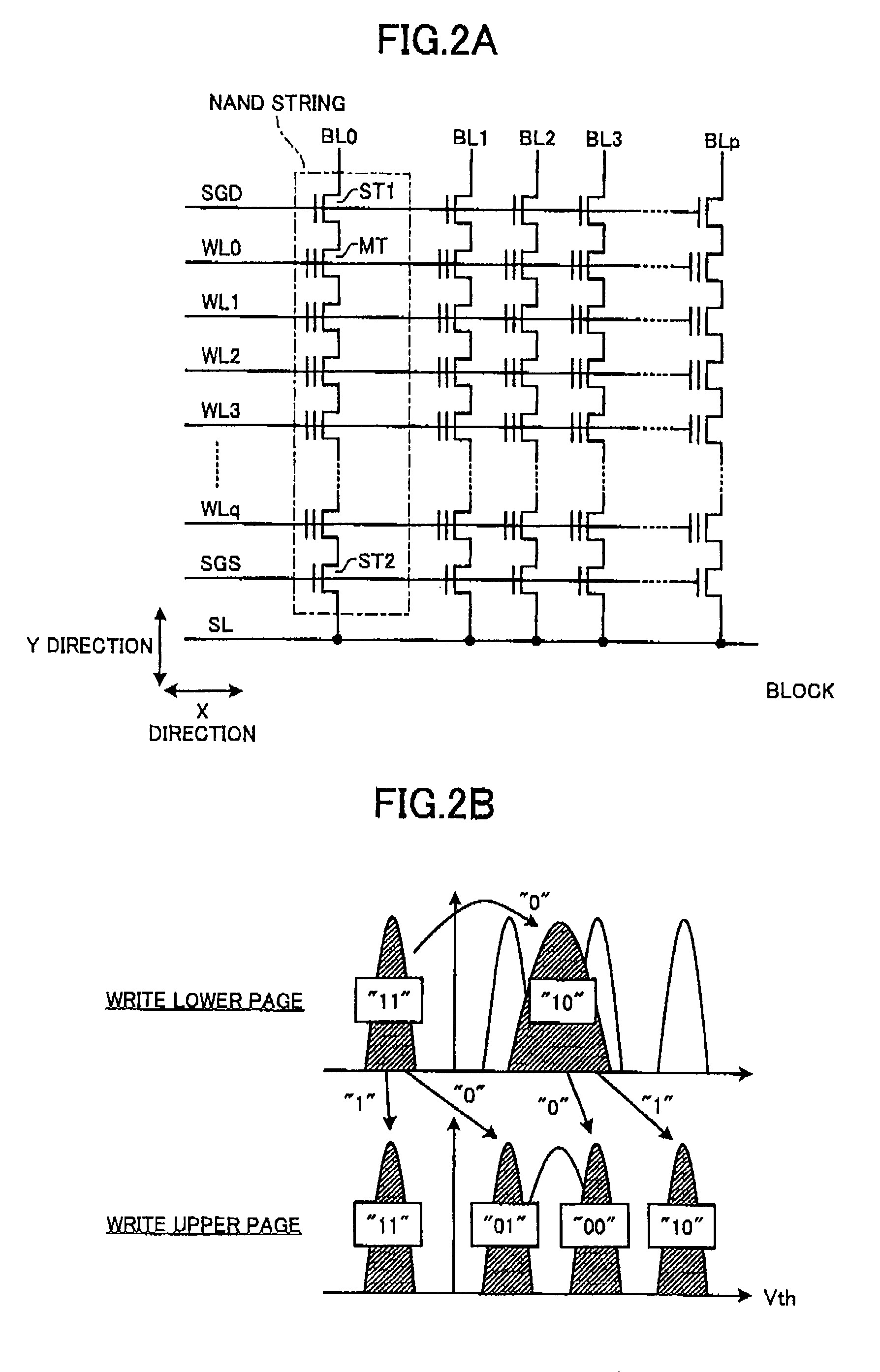
[0059]Physical page: A unit that can be collectively written and read out in a NAND memory chip. A physical page size is, for example, 4 kB. However, a redundant bit such as an error correction code added to main data (user data, etc.) in an SSD is not included. Usually, 4 kB+redundant bit (e.g., several 10 B) is a unit simultaneously written in a memory cell. However, for convenience of explanation, the physical page is defined as explained above.

[0060]Logical page: A writing and readout unit set in the SSD. The logical page is associated with one or more physical pages. A logical page size is, for example, 4 kB in an 8-bi...

first embodiment

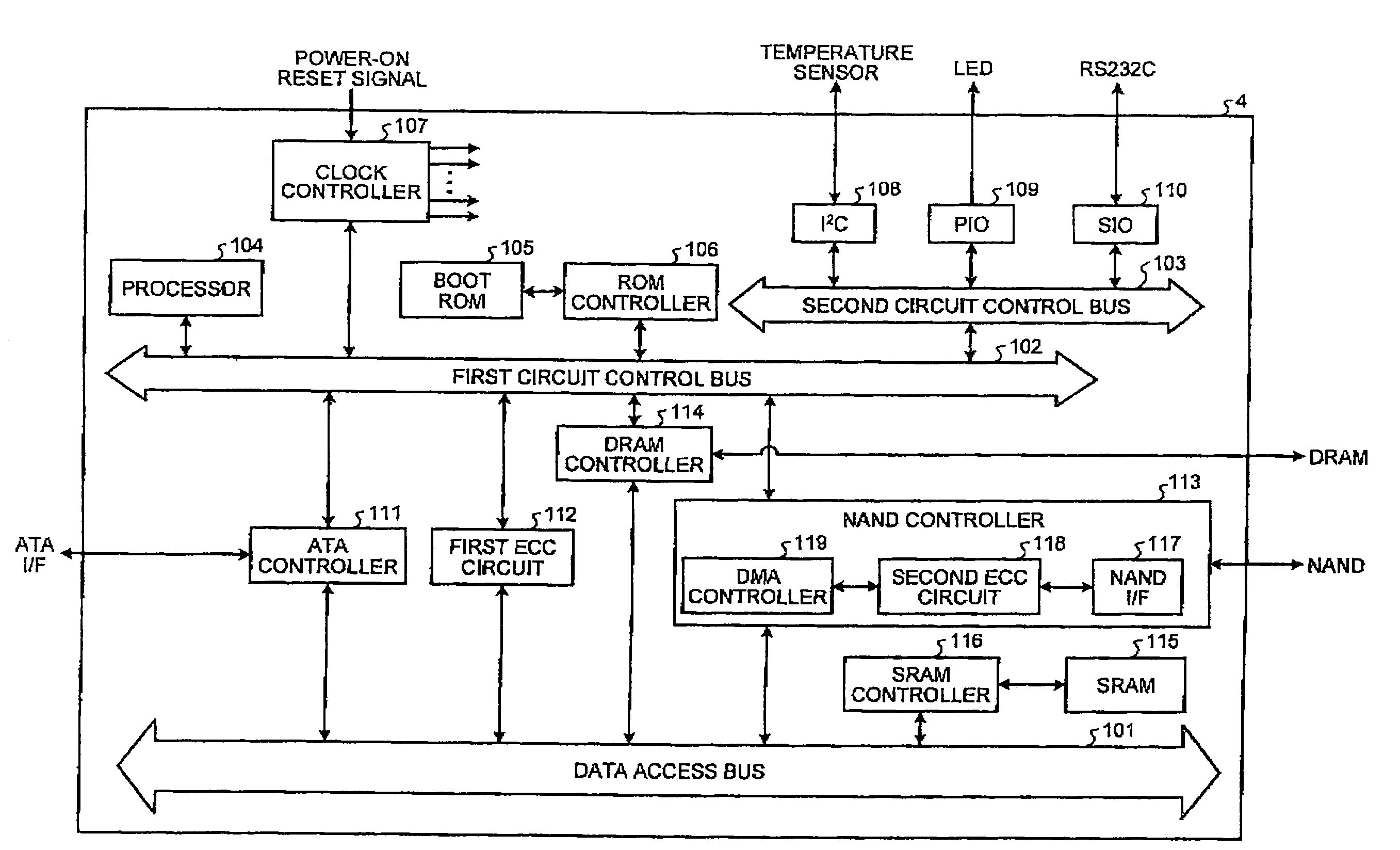
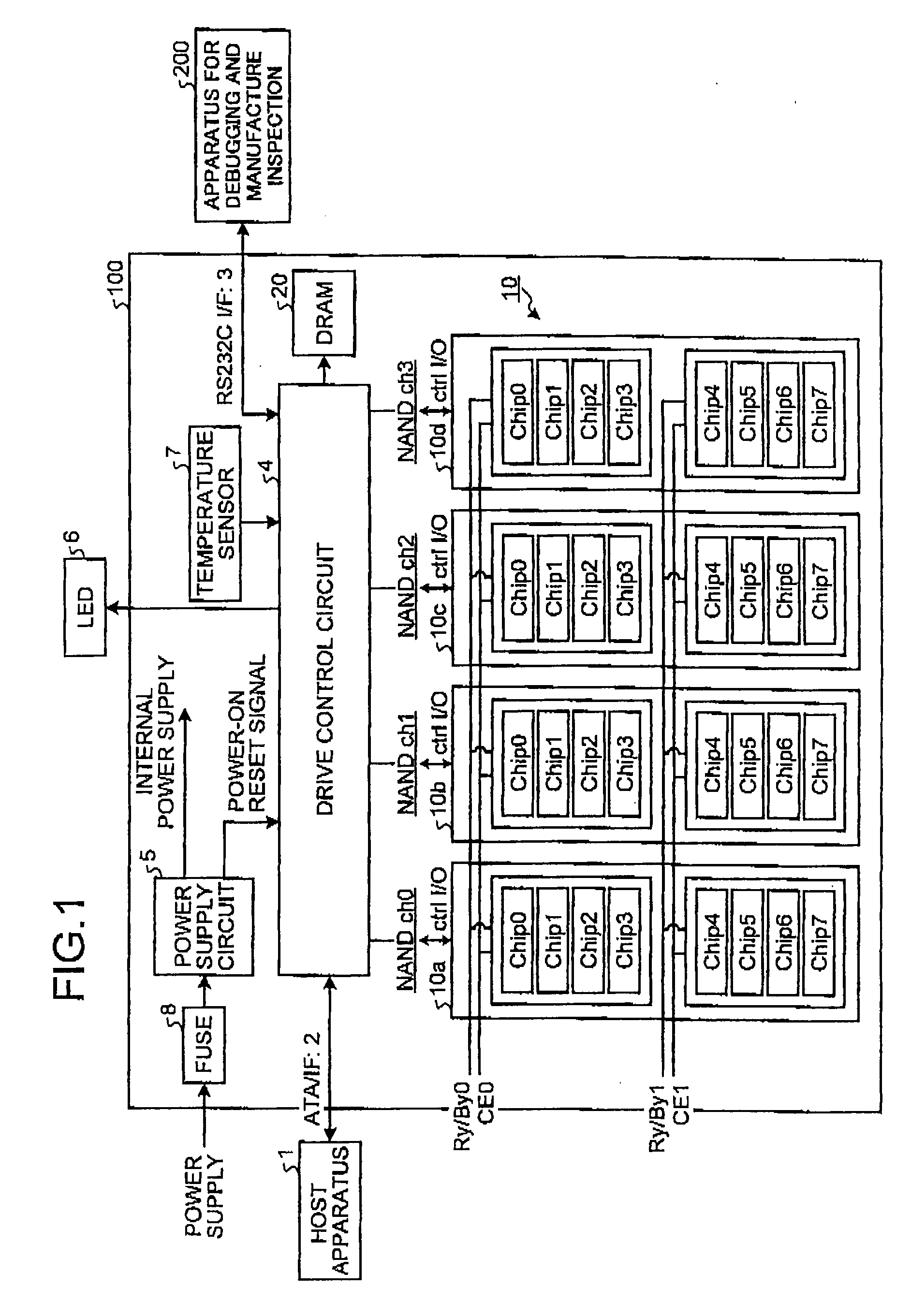
[0074]FIG. 1 is a block diagram of a configuration example of an SSD (Solid State Drive) 100. The SSD 100 is connected to a host apparatus 1 such as a personal computer or a CPU core via a memory connection interface such as an ATA interface (ATA I / F) 2 and functions as an external storage of the host apparatus 1. The SSD 100 can transmit data to and receive data from an apparatus for debugging and manufacture inspection 200 via a communication interface 3 such as an RS232C interface (RS232C I / F). The SSD 100 includes a NAND-type flash memory (hereinafter abbreviated as NAND memory) 10 as a nonvolatile semiconductor memory, a drive control circuit 4 as a controller, a DRAM 20 as a volatile semiconductor memory, a power supply circuit 5, an LED for state display 6, a temperature sensor 7 that detects the temperature in a drive, and a fuse 8.

[0075]The power supply circuit 5 generates a plurality of different internal DC power supply voltages from external DC power supplied from a powe...

second embodiment

[0363]FIG. 22 shows a perspective view of an example of a personal computer. A personal computer 1200 includes a main body 1201 and a display unit 1202. The display unit 1202 includes a display housing 1203 and a display device 1204 accommodated in the display housing 1203.

[0364]The main body 1201 includes a chassis 1205, a keyboard 1206, and a touch pad 1207 as a pointing device. The chassis 1205 includes a main circuit board, an ODD unit (Optical Disk Device), a card slot, and the SSD 1100 described in the first embodiment.

[0365]The card slot is provided so as to be adjacent to the peripheral wall of the chassis 1205. The peripheral wall has an opening 1208 facing the card slot. A user can insert and remove an additional device into and from the card slot from outside the chassis 1205 through the opening 1208.

[0366]The SSD 1100 may be used instead of the prior art HDD in the state of being mounted in the personal computer 1200 or may be used as an additional device in the state of...


PUM


Abstract

A system includes: a first input buffer that functions as an input buffer for a third storing area; and a second input buffer that functions as an input buffer for the third storing area and that separately stores data with a high update frequency for the third storing area. In the system, a plurality of data written in a first storing area or a second storing area are flushed to the first input buffer in units of logical blocks. Also, a plurality of data written in the first input buffer are relocated to the third storing area in units of logical blocks.

Description

CROSS-REFERENCE TO RELATED APPLICATIONS[0001]This application is based upon and claims the benefit of priority from the prior Japanese Patent Application No. 2008-51475, filed on Mar. 1, 2008 and the prior Japanese Patent Application No. 2008-63404, filed on March 12; the entire contents of which are incorporated herein by reference.BACKGROUND OF THE INVENTION[0002]1. Field of the Invention[0003]The present invention relates to a memory system including a nonvolatile semiconductor memory.[0004]2. Description of the Related Art[0005]The SSD includes a plurality of flash memory chips, a controller that performs read / write control for the respective flash memory chips in response to a request from a host apparatus, a buffer memory for performing data transfer between the respective flash memory chips and the host apparatus, a power supply circuit, and a connection interface to the host apparatus (for example, Japanese Patent No. 3688835).[0006]Examples of the nonvolatile semiconductor ...

Claims


Application Information

Patent Timeline
Patent Type & Authority Applications(United States)
IPC IPC(8): G06F12/00G06F12/02G06F12/08
CPCG06F12/0246G06F2212/7203G06F12/0866G11C16/02G11C16/06G11C16/10
Inventor YANO, JUNJIMATSUZAKI, HIDENORIHATSUDA, KOSUKEOKAMOTO, WATARUKATO, RYOICHI
Owner KK TOSHIBA
Why Eureka
Try Eureka