Electron microscopy

a technology of electron microscopy and electron microscopy, which is applied in the field of electron microscopy, can solve the problems of not offering sufficient discrimination and no longer meeting the needs of analysis, and achieve the effect of improving the degree of operation

Inactive Publication Date: 2009-10-01
HITACHI HIGH-TECH CORP
View PDF7 Cites 23 Cited by
  • Summary
  • Abstract
  • Description
  • Claims
  • Application Information

AI Technical Summary

Benefits of technology

[0016]According to the present invention, discrimination of the backscattered electrons and the transmission electrons can be performed at any scattering angle. Accordingly, it is possible to obtain the backscattered electron image and the scanning transmission electron image on the basis of discrimination at appropriate scattering angles even when thickness, inclination, and compositio

Problems solved by technology

However, such conventional methods cannot offer sufficient discrimin

Method used


Image

  • Electron microscopy
  • Electron microscopy
  • Electron microscopy

Examples


Embodiment Construction

[0028]Hereinafter, with reference to the drawings, an embodiment of the present invention will be described in detail.

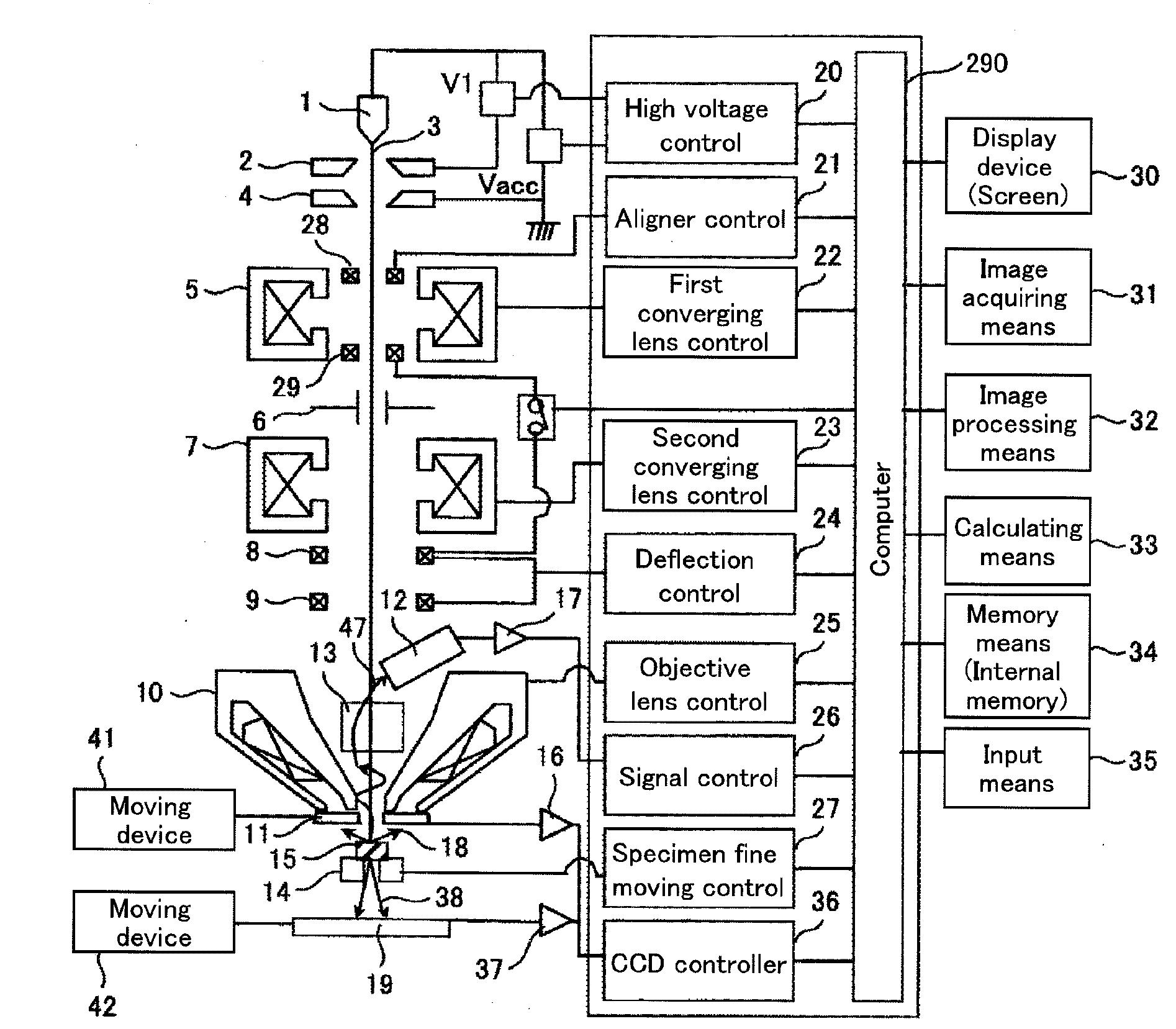
[0029]FIG. 1 is a schematic diagram of the embodiment of the present invention.

[0030]A primary electron beam 3 is discharged from a cathode 1 by a voltage V1 applied to the cathode 1 and a first electrode 2, and is accelerated by a voltage Vacc applied to a second electrode 4 to advance to an electromagnetic lens system at a rear stage.

[0031]The acceleration voltage Vacc and the V1 are controlled by a high voltage control circuit 20. The primary electron beam 3 is converged by a first converging lens 5 controlled by a first converging lens control circuit 22. Here, the specimen irradiation current of the primary electron beam 3 is restricted by an objective lens aperture 6. In order for the center of the electron beam to pass through a hole center of the objective lens aperture 6, an electron-beam center-axis adjustment aligner 28, an aligner control circuit 21, and ...


PUM


Abstract

Using, as a detector, a CCD detector having a CCD element to which a scintillator is closely fixed, a backscattered or scanning transmission image is obtained by the following method. The detector is disposed directly under an objective lens to obtain the backscattered electron image. When one point of a specimen is irradiated with an electron beam, backscattered or transmission electrons generated from the specimen collide with the scintillator to form a luminescent pattern. This pattern is detected by the CCD detector, and stored in a memory. This processing is sequentially repeated for each irradiation position to obtain all the patterns in an electron beam scanning range. Arithmetic processing is performed on each pattern to convert it into an image. Usually, image data for one pixel is calculated from one pattern. By sequentially repeating this, a backscattered or transmission electron image in the electronic beam scanning range can be obtained.

Description

BACKGROUND OF THE INVENTION[0001]1. Field of the Invention[0002]The present invention relates to an electron microscopy employing a CCD detector in order to acquire a backscattered electron image, a transmission electron image, or a scanning transmission electron image.[0003]2. Description of the Related Art[0004]When an electron beam enters a specimen in an electron microscopy, a part of the electron beam is scattered at a large angle by an atom in the specimen. Then, the scattered electron beam discharges electrons (backscattered electrons) from the surface of the specimen while losing little energy. Another part of the electron beam discharges electrons (transmission electrons) behind the specimen, without being absorbed in the specimen.[0005]The backscattered electrons can be mainly classified into two types: high angle backscattered electrons scattered at high angles from the surface of the specimen and low angle backscattered electrons scattered at low angles from the surface ...

Claims


Application Information

Patent Timeline
IPC IPC(8): H01J3/14
CPCH01J37/222H01J37/244H01J37/28H01J2237/24485H01J2237/2443H01J2237/24455H01J2237/24475H01J2237/221
Inventor HOSOYA, KOTARONAKAYAMA, YOSHIHIKONAGAOKI, ISAO
Owner HITACHI HIGH-TECH CORP
Why Eureka
Try Eureka