Method for manufacturing multilayer printed wiring board

a multi-layer printed, wiring board technology, applied in the direction of final product manufacturing, sustainable manufacturing/processing, semiconductor/solid-state device details, etc., can solve the problems of undesirable electrical characteristics and possible malfunction of the ic chip

Active Publication Date: 2009-10-01
IBIDEN CO LTD
View PDF1 Cites 70 Cited by
  • Summary
  • Abstract
  • Description
  • Claims
  • Application Information

AI Technical Summary

Benefits of technology

[0006]An object of the present invention is to propose a method for manufacturing a multilayer printed wiring board capable of making proper connection to the terminal of a built-in electronic component.

Problems solved by technology

Since lead components of this type can be cut off and corroded, they may be disconnected from the IC chip and the IC chip may malfunction.
Further, when the chip capacitor is surface-mounted, the wiring length thereof to the IC chip is increased, which may cause undesirable electrical characteristics.

Method used


Image

  • Method for manufacturing multilayer printed wiring board
  • Method for manufacturing multilayer printed wiring board
  • Method for manufacturing multilayer printed wiring board

Examples


first embodiment

Modified Example of First Embodiment

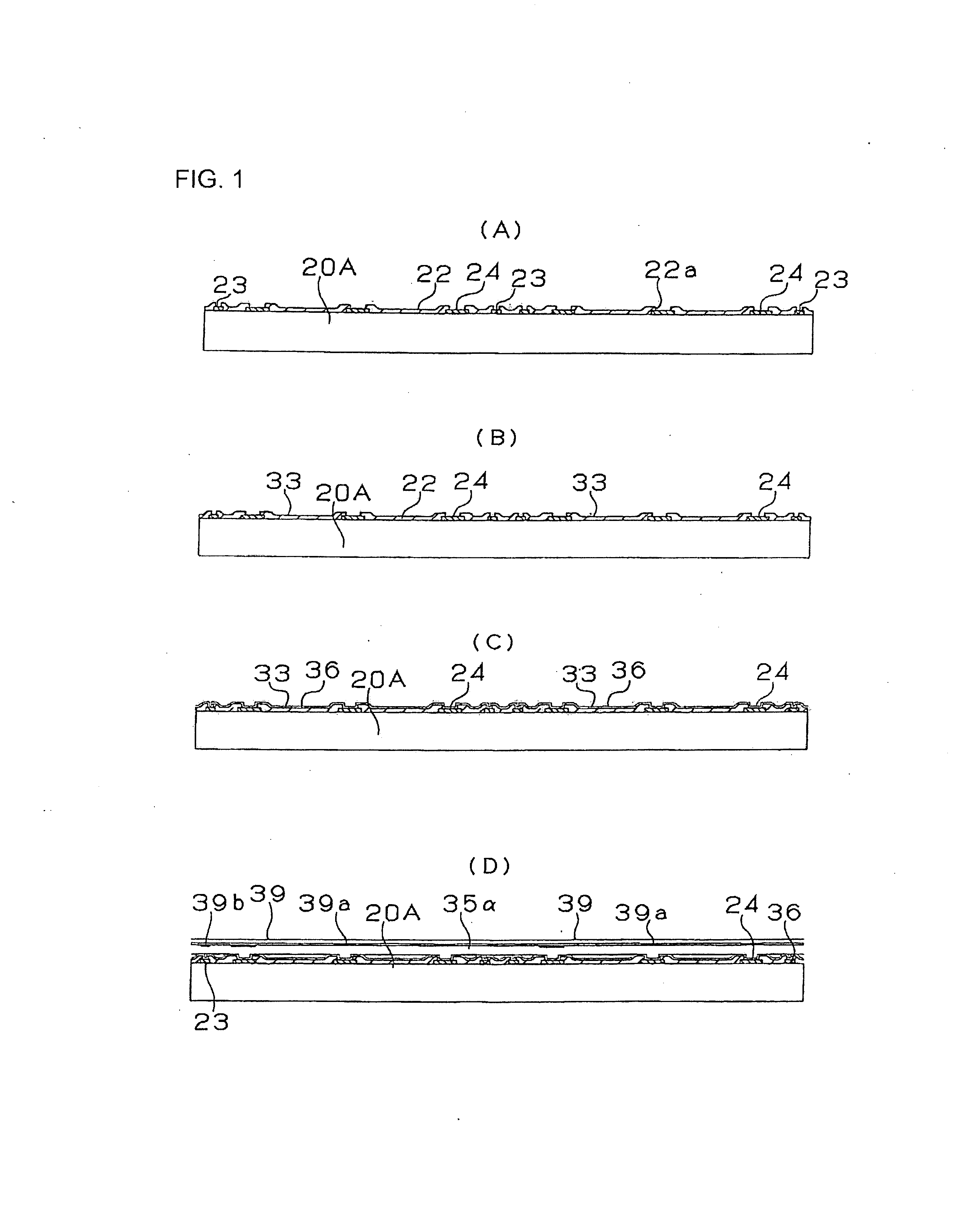
[0068]A method for manufacturing a printed wiring board according to a modified example of the first embodiment will be described referring to FIG. 8. In the first embodiment, the resin tape is disposed on the bottom surface of the through bore 32 of the substrate. In the modified example of the first embodiment, a copper foil is employed in place of the resin tape.

[0069]The through bore 32 is formed, and a copper foil 27 as thick as the conductor circuit 28 on the back surface side is disposed on a bottom side (FIGS. 8A to 8C). Then, an adhesive 29 is coated on the copper foil 27, and the IC chip 20 is accommodated (FIGS. 8D and 8E). Since the subsequent steps are the same as those of the first embodiment, the explanation thereof is omitted. In the modified example of the first embodiment, since the copper foil 27 as thick as the conductor circuit 28 on the back surface side is used, the modified example can more increase the positioning accuracy...

second embodiment

[0070]Subsequently, a multilayer printed wiring board according to a second embodiment of the present invention will be described referring to FIG. 11.

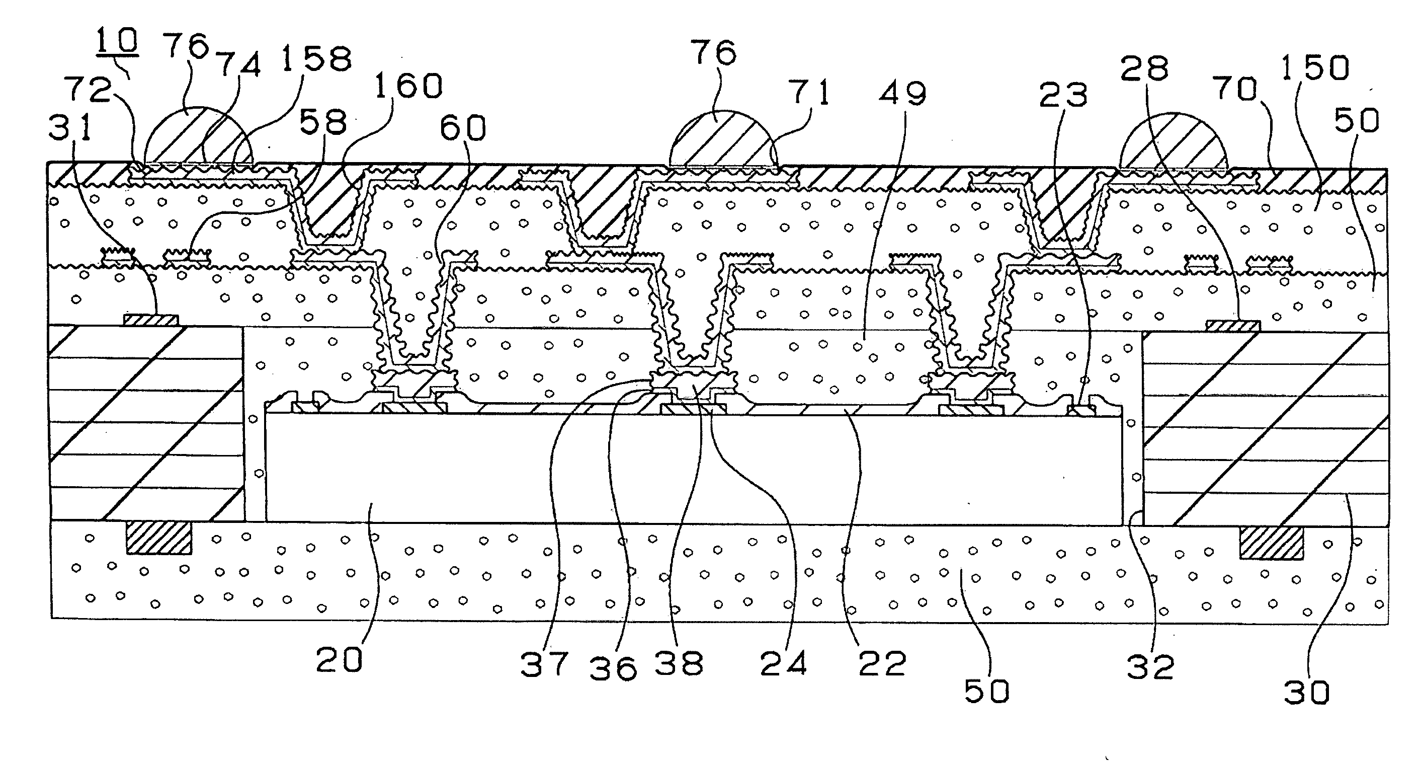
[0071]In the first embodiment described above, the IC chip is accommodated in the multilayer printed wiring board. In contrast, in the second embodiment, a chip capacitor 120 is accommodated in a multilayer printed wiring board 10, and an IC chip 140 is mounted above the surface of the multilayer printed wiring board 10. The multilayer printed wiring board 10 is mounted on a daughter board 90.

[0072]Each power supply pad 144P of the IC chip 140 is connected to each terminal 124 of the chip capacitor 120 through via-hole 60-conductor circuit 58-via-hole 160-conductor circuit 158-solder bump 76U on the upper surface side of a core substrate 30. Each terminal 124 of the chip capacitor 120 is connected to each power supply pad 94P of the daughter board 90 through via-hole 60-conductor circuit 58-via-hole 160-conductor circuit 158-solder bu...

third embodiment

[0083]A multilayer printed wiring board according to a third embodiment of the present invention will be described referring to FIG. 15.

[0084]The multilayer printed wiring board of the third embodiment is accommodated in an insulation resin substrate (core substrate) 30. A rewiring layer composed of a resin layer 80, via-holes 82, and a conductor circuit 84 is formed on an IC chip 20. An insulation resin layer 250 and columnar electrodes 260 are formed on the conductor circuit 84 constituting the redistribution layer. Further, a resin insulation layer 150, to which via-holes 160 and a conductor circuit 158 are formed, is disposed on the columnar electrode 260. Solder bumps 76 are disposed to the openings 71 of a solder resist layer 70 on the resin insulation layer 150.

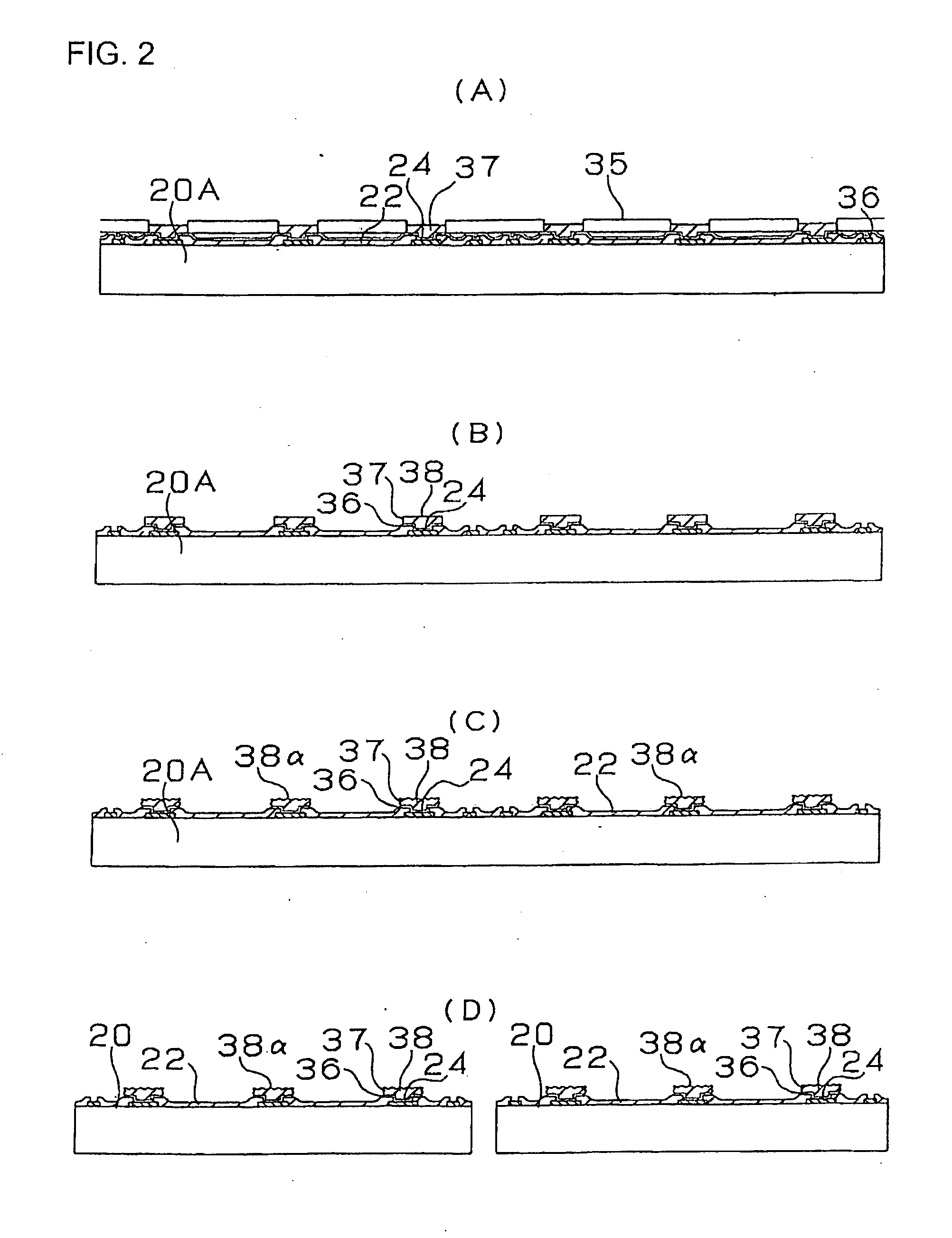
[0085]A method for manufacturing the multilayer printed wiring board of the third embodiment will be described referring to FIGS. 12 to 14.

[0086]The IC chip 20, to which the redistribution layer composed of the resin l...


PUM

PropertyMeasurementUnit
diameteraaaaaaaaaa
diameteraaaaaaaaaa
thicknessaaaaaaaaaa

Abstract

A method for manufacturing a multilayer printed wiring board having an electronic component housed therein includes forming a first conductor circuit on a first surface of a substrate. A first alignment mark is formed on the first surface of the substrate separate from the conductor circuit and forming a through bore in the substrate, the through bore extending from the first surface of the substrate to a second surface of the substrate. A seal member is disposed on the second surface of the substrate, the seal member sealing an opening on the second surface of the through bore to provide a sealed through bore. An electronic component is inserted in the sealed through bore using the first alignment mark on the first surface of the substrate.

Description

CROSS-REFERENCE TO RELATED APPLICATIONS[0001]The present application claims the benefits of priority to U.S. Application Nos. 61 / 040,011, filed Mar. 27, 2008 and 61 / 094,096 filed Sep. 4, 2008. The contents of those applications are incorporated herein by reference in their entirety.BACKGROUND OF THE INVENTION[0002]1. Field of Invention[0003]The present invention relates to a method for manufacturing a build-up multilayer printed wiring board, and more particularly to a method for manufacturing a multilayer printed wiring board having electronic components such as active devices such as an IC chip and passive devices such as a chip capacitor built therein.[0004]2. Discussion of the Background[0005]Integrated circuit (IC) chips have been electrically connected to a printed wiring board by a mounting method such as wire bonding, tape automated bonding (TAB), and a flip chip. Further, chip capacitors have been surface-mounted on a substrate. In the method for mounting the IC chip, the I...

Claims


Application Information

Patent Timeline
Patent Type & Authority Applications(United States)
IPC IPC(8): H05K1/18H05K3/10H05K3/30H05K3/42
CPCH01L23/5389Y10T29/49165H01L24/25H01L24/82H01L2223/54426H01L2223/5448H01L2223/54486H01L2224/16225H01L2224/24227H01L2224/2518H01L2224/82039H01L2924/01004H01L2924/01005H01L2924/01011H01L2924/01012H01L2924/01018H01L2924/01027H01L2924/01029H01L2924/0103H01L2924/01033H01L2924/01046H01L2924/01057H01L2924/01074H01L2924/01078H01L2924/01079H01L2924/01082H01L2924/14H01L2924/15153H01L2924/1517H01L2924/18162H01L2924/19041H05K1/0231H05K1/0269H05K1/185H05K3/0035H05K3/4602H05K3/4644H05K2201/0187H05K2201/09918H05K2201/10636H05K2201/10674H05K2201/10727H05K2203/1469H05K2203/166H01L24/24Y10T29/4913Y10T29/49139Y10T29/49126H01L2924/01006H01L2924/01019H01L2924/01024H01L2924/01047H01L2924/12042H01L2224/05027H01L2224/05024H01L2224/05008H01L2224/05568H01L2224/05001H01L2224/05147H01L24/19H01L24/20Y02P70/50H01L2924/00H01L2924/00014
Inventor TANAKA, HIRONORI
Owner IBIDEN CO LTD
Why Eureka
Try Eureka