Super junction semiconductor device

a semiconductor device and super junction technology, applied in the field of super junction semiconductor devices, can solve the problems of reducing the feature size without affecting the device characteristics, affecting the most important device parameters, and reducing the auto-doping phenomenon, so as to reduce the auto-doping phenomenon, increase the doping concentration, and shrink the column width

Inactive Publication Date: 2009-10-08
INERGY TECH
View PDF4 Cites 2 Cited by
  • Summary
  • Abstract
  • Description
  • Claims
  • Application Information

AI Technical Summary

Benefits of technology

[0012]Accordingly, a silicon dioxide layer is inserted between the P-type and N-type layers of the super junction to reduce auto doping phenomenon, at the same time using the principle of charge compensation to reach fully depletion and break the silicon limit. The silicon dioxide layer can block the impurities di

Problems solved by technology

However, there are still several drawbacks of conventional super junction devices.
The major drawback is that while the development of conventional super junction devices to obtain the best trade-off between the reverse blocking voltage and specific on-resistance is hard to achieve, besides that shrinking the feature size without affecting the device characteristics is also difficult.
Because conventional super junction devices suffer sever auto-doping effect after thermal

Method used


Image

  • Super junction semiconductor device
  • Super junction semiconductor device
  • Super junction semiconductor device

Examples


Embodiment Construction

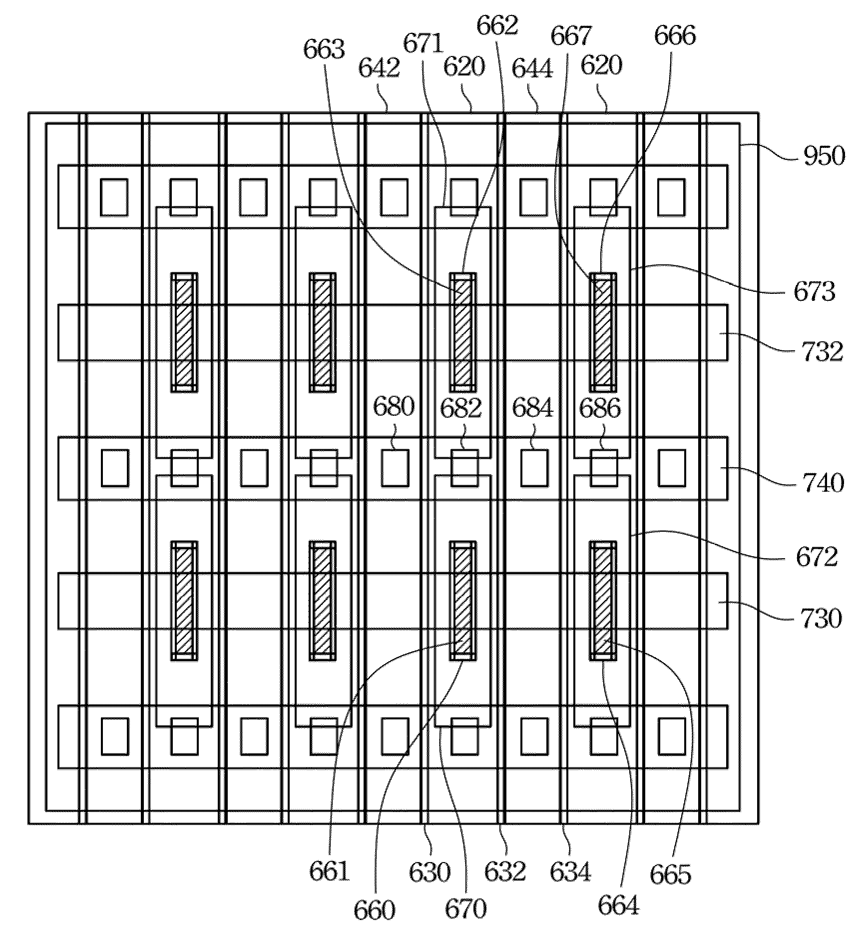
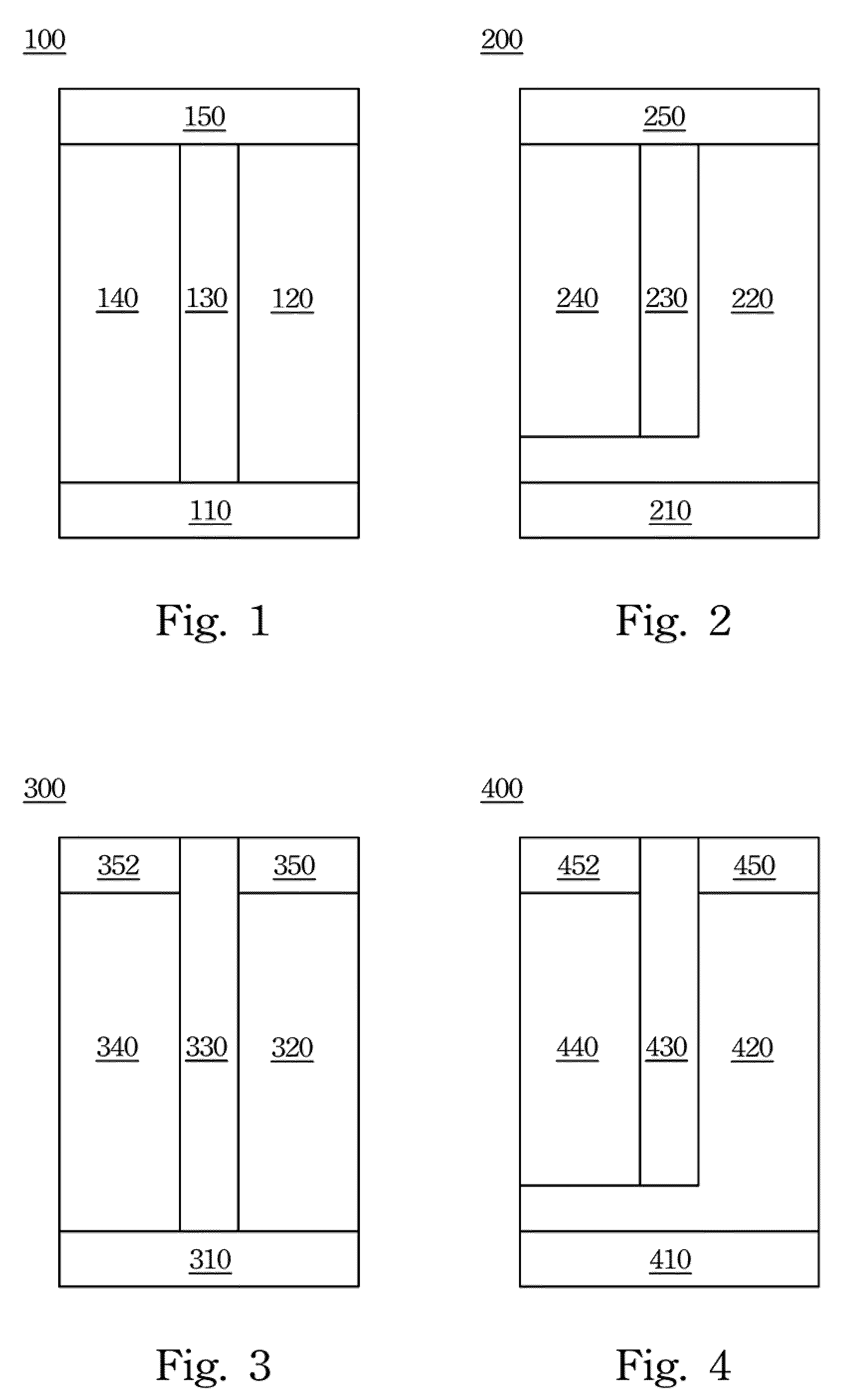
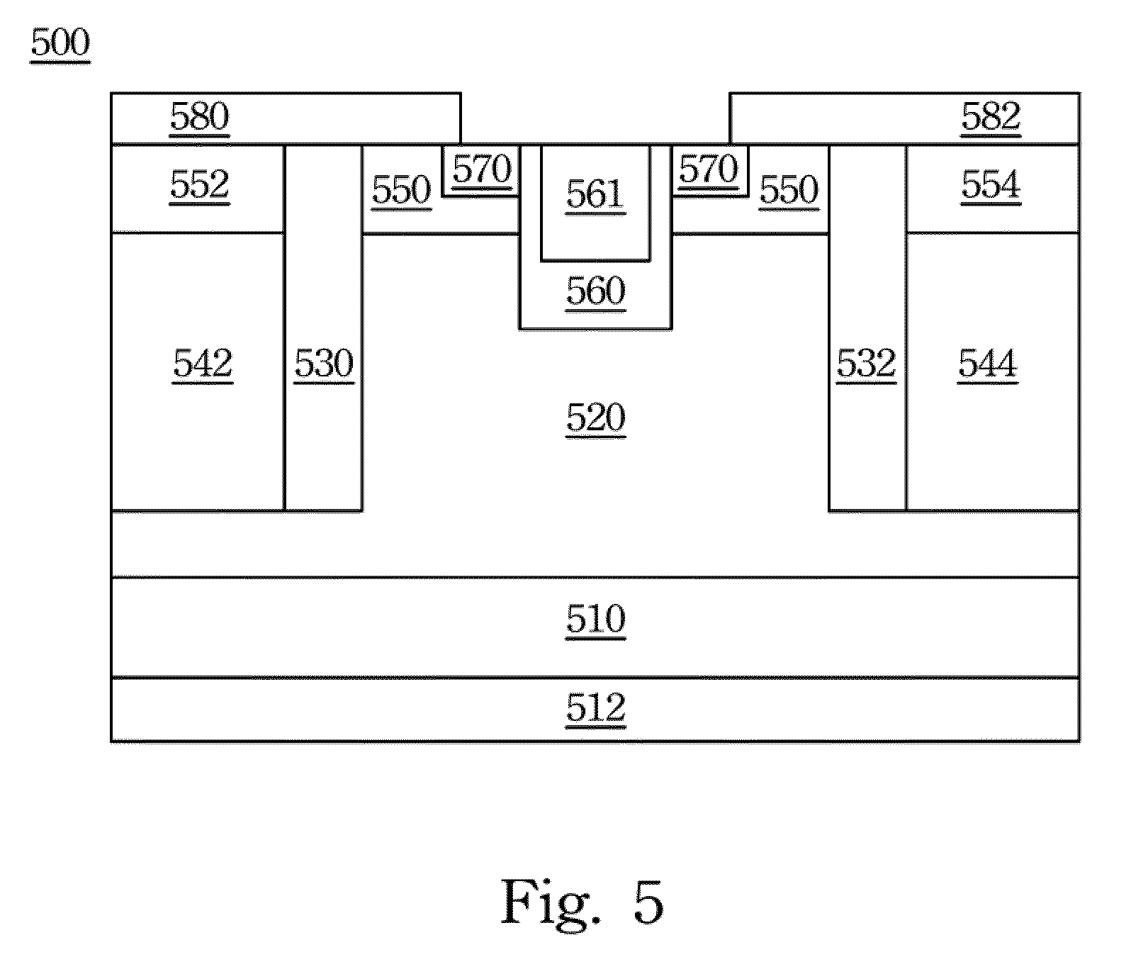
[0025]Reference will now be made in detail to the present preferred embodiments of the invention, examples of which are illustrated in the accompanying drawings. Wherever possible, the same reference numbers are used in the drawings and the description to refer to the same or like parts.

[0026]It will be understood that, although the terms first, second, etc. may be used herein to describe various elements, these elements should not be limited by these terms. These terms are only used to distinguish one element from another. For example, a first element could be termed a second element, and, similarly, a second element could be termed a first element, without departing from the scope of the example embodiments. As used herein, the term “and / or” includes any and all combinations of one or more of the associated listed items.

[0027]It will be understood that when an element is referred to as being “connected” or “coupled” to another element, it can be directly connected or coupled to th...


PUM


Abstract

In the specification and drawing a super junction semiconductor device is disclosed. The super junction semiconductor device comprises a P-type layer, a N+ substrate, a N-type layer, a silicon dioxide layer and a P+ layer. The N+ substrate is disposed under the P-type layer. The N-type layer is disposed on the N+ substrate. The silicon dioxide layer is disposed between the N-type layer and the P-type layer. The P+ layer is disposed on the P-type layer and the N-type layer.

Description

RELATED APPLICATIONS[0001]This application claims priority to American Provisional Application Ser. No. 61 / 064,973, filed Apr. 7, 2008, which is herein incorporated by reference.BACKGROUND[0002]1. Field of Invention[0003]The present invention is related to a semiconductor device. More particularly, the present invention relates to a super junction semiconductor device.[0004]2. Description of Related Art[0005]Power semiconductor devices are used in many fields such as home electric appliance, automobile, electric train and electric transmission. Power semiconductor devices are applied to inverter systems and power supply circuits as switching mode devices. In these applications, under specific reverse blocking capability, lowering the specific on-resistance of power semiconductor device is necessary for reducing power losses in the systems. There had several versions of power semiconductor devices been published, such as planar gate MOSFET, trench gate MOSFET, lateral MOSFET and Vert...

Claims


Application Information

Patent Timeline
IPC IPC(8): H01L29/68
CPCH01L29/0634H01L29/0649H01L29/7813H01L29/0696H01L29/1095H01L29/0653
Inventor LIN, MING-JANG
Owner INERGY TECH
Why Eureka
Try Eureka