Semiconductor device and method of manufacturing the same

Active Publication Date: 2009-10-08
SHINKO ELECTRIC IND CO LTD
View PDF5 Cites 31 Cited by
  • Summary
  • Abstract
  • Description
  • Claims
  • Application Information

AI Technical Summary

Benefits of technology

[0015]An object of the present invention is to provide a semiconductor device and a method of manufacturing the same, which satisfies, when needed, a need to increase the

Problems solved by technology

Accordingly, a disadvantage of the package becoming “warp

Method used


Image

  • Semiconductor device and method of manufacturing the same
  • Semiconductor device and method of manufacturing the same
  • Semiconductor device and method of manufacturing the same

Examples


Example

[0026]Description is given below of preferred embodiments of the present invention with reference to the accompanying drawings.

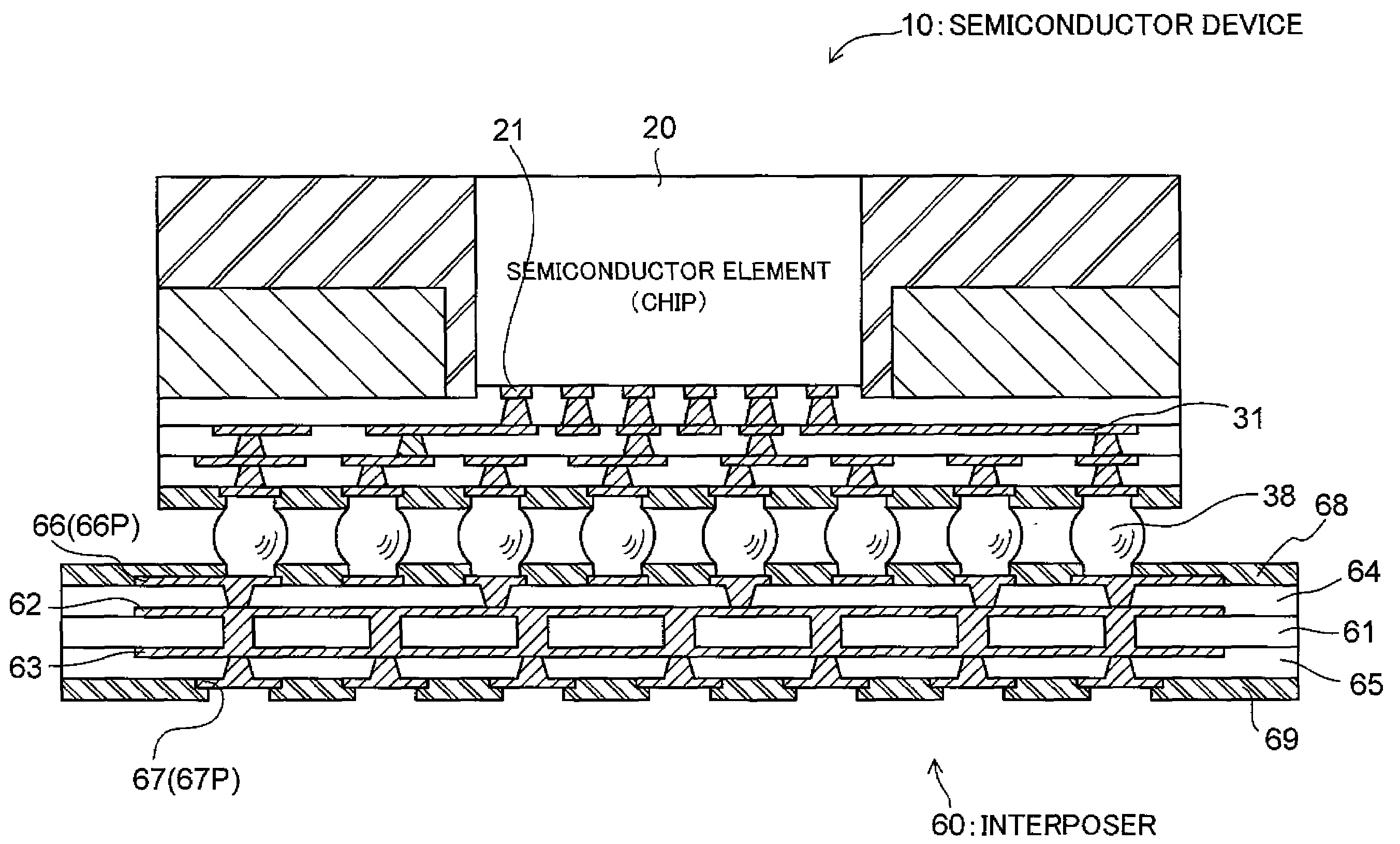
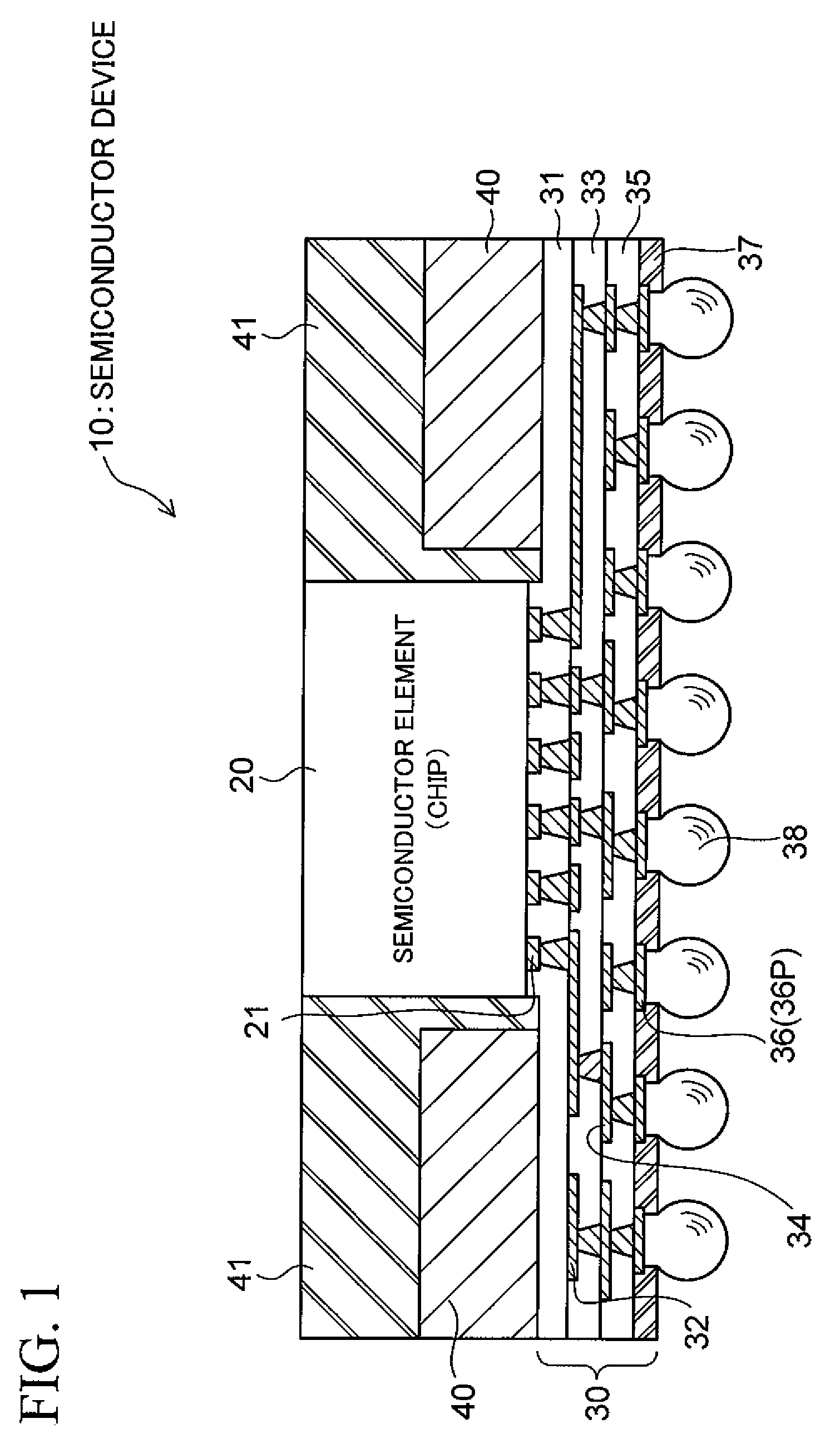
[0027]FIG. 1 shows in sectional view the configuration of a semiconductor device provided with a package having a fan-out structure according to one embodiment of the present invention.

[0028]A semiconductor device 10 according to the embodiment of the present invention is basically provided with a chip 20 (typically, a silicon (Si) chip) such as a semiconductor element, a laminated wiring structure 30 provided integrally with the chip 20, a frame 40 disposed on the laminated wiring structure 30 to surround the periphery of the side surface of the chip 20, and a sealing resin 41 formed to coat the overall surface of the frame 40 and the periphery of the side surface of the chip 20 (or to bury the overall chip 20 therein).

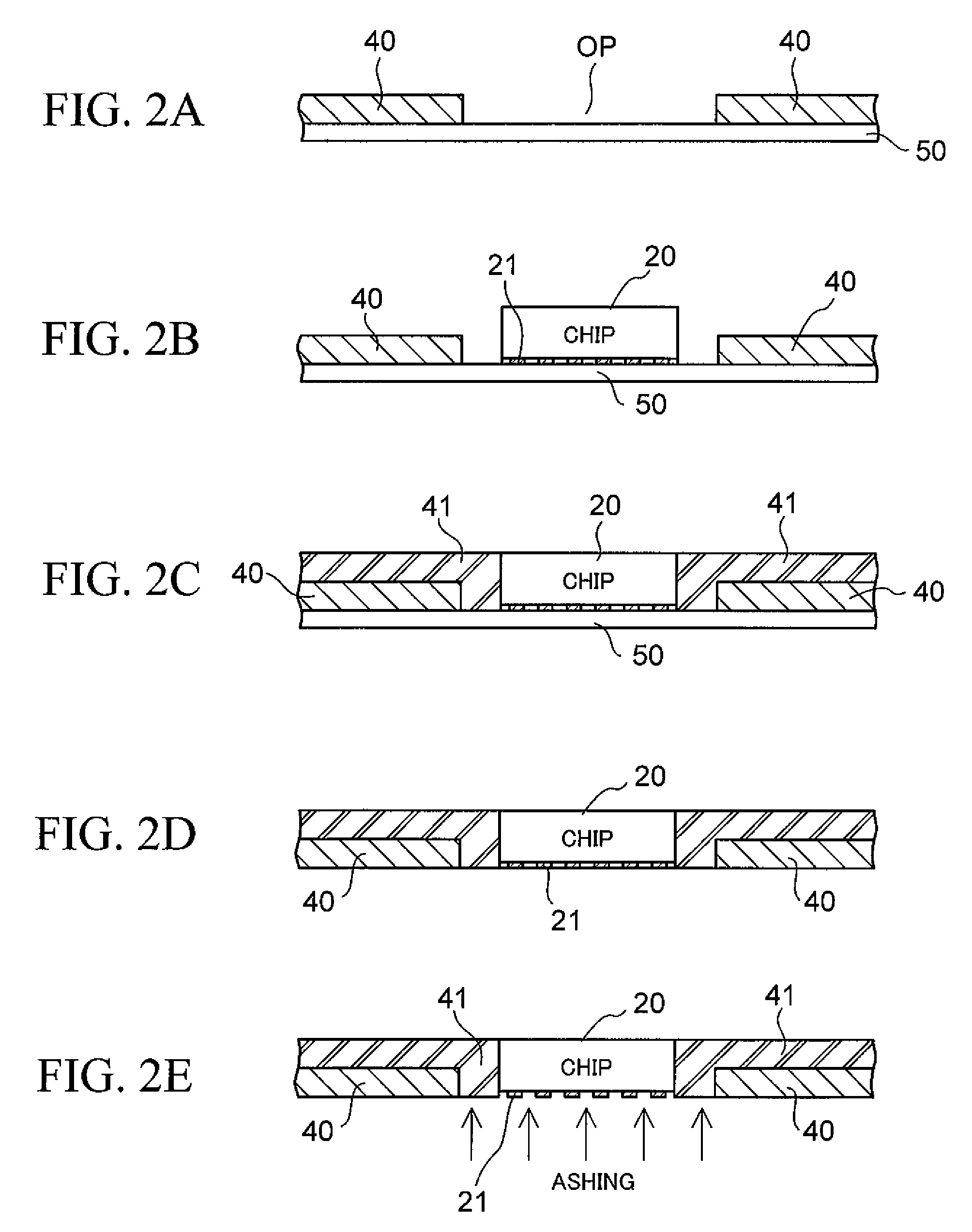
[0029]The semiconductor chip 20 built in the semiconductor device 10 is a chip (also referred to as “die”) obtained by dicing, in units of d...


PUM


Abstract

A semiconductor device includes a chip, a laminated wiring structure formed integrally with the chip, a frame disposed to surround the chip and made of a material having stiffness, and a sealing resin formed to bury therein the frame and at least the periphery of the side surface of the chip. The laminated wiring structure includes a required number of wiring layers, which are formed by patterning in such a manner that a wiring pattern directly routed from an electrode terminal of the chip is electrically connected to pad portions for bonding external connection terminals, the pad portions being provided, at a position directly below a mounting area of the chip and at a position directly below an area outside the mounting area, on a surface to which the external connection terminals are bonded.

Description

CROSS-REFERENCE TO RELATED APPLICATIONS[0001]This application is based on and claims priority of Japanese Patent Application No. 2008-96800 filed on Apr. 3, 2008, the entire contents of which are incorporated herein by reference.BACKGROUND OF THE INVENTION[0002](a) Field of the Invention[0003]The present invention relates to a semiconductor device and a method of manufacturing the same, and more particularly to a semiconductor device having a wiring board for use in mounting a semiconductor element or the like, and a method of manufacturing the same.[0004]Note that the “wiring board” is hereinafter also referred to as a “semiconductor package” or merely a “package” for the sake of convenience, because the wiring board plays the role of mounting a semiconductor element or the like thereon.[0005](b) Description of the Related Art[0006]A semiconductor package such as a ball grid array (BGA), a land grid array (LGA) or a pin grid array (PGA) generally has a multilayer wiring structure. ...

Claims


Application Information

Patent Timeline
IPC IPC(8): H01L23/02H01L21/50
CPCH01L21/568H01L2224/12105H01L23/16H01L23/3128H01L23/49816H01L23/5389H01L23/544H01L24/19H01L24/20H01L2223/54426H01L2223/54473H01L2224/04105H01L2224/20H01L2924/01011H01L2924/01013H01L2924/01015H01L2924/01029H01L2924/01078H01L2924/01079H01L2924/01082H01L2924/14H01L2924/15311H01L2924/18161H01L2924/18162H01L2924/01005H01L2924/01006H01L2924/01024H01L2924/01033H01L2924/10253H01L21/6835H01L2224/0401H01L2924/00H01L2224/96H01L2924/15788H01L2924/181
Inventor ARAI, TADASHI
Owner SHINKO ELECTRIC IND CO LTD
Why Eureka
Try Eureka