Reliability improvement in a compound semiconductor mmic

Inactive Publication Date: 2009-10-08
NORTHROP GRUMMAN SYST CORP
View PDF8 Cites 8 Cited by
  • Summary
  • Abstract
  • Description
  • Claims
  • Application Information

AI Technical Summary

Benefits of technology

[0022]The present invention also provides a technique to increase the life of the die attachment systems when thermo-mechanical metal fatigue occurs in the die attachment metallization first.
[0023]The present invention significantly reduces the mechanical strain by reducing the die attachment area of the MMIC (the larger the die attachment area, the higher the mechanical strain), keeping only that portion that is needed for mechanical stability, electrical conductivity, and thermal dissipation of the active device. This yields a device with an effectively smaller die attachment area that

Problems solved by technology

Further, known manufacturing methods utilize 100% of the back of the MMIC for die attachment which will in real

Method used


Image

  • Reliability improvement in a compound semiconductor mmic
  • Reliability improvement in a compound semiconductor mmic
  • Reliability improvement in a compound semiconductor mmic

Examples


Embodiment Construction

[0032]So that the manner in which the above recited features, advantages and objects of the present invention are attained can be understood in detail, more particular description of the invention, briefly summarized above, may be had by reference to the embodiment thereof that is illustrated in the appended drawings. In all the drawings, identical numbers represent the same elements.

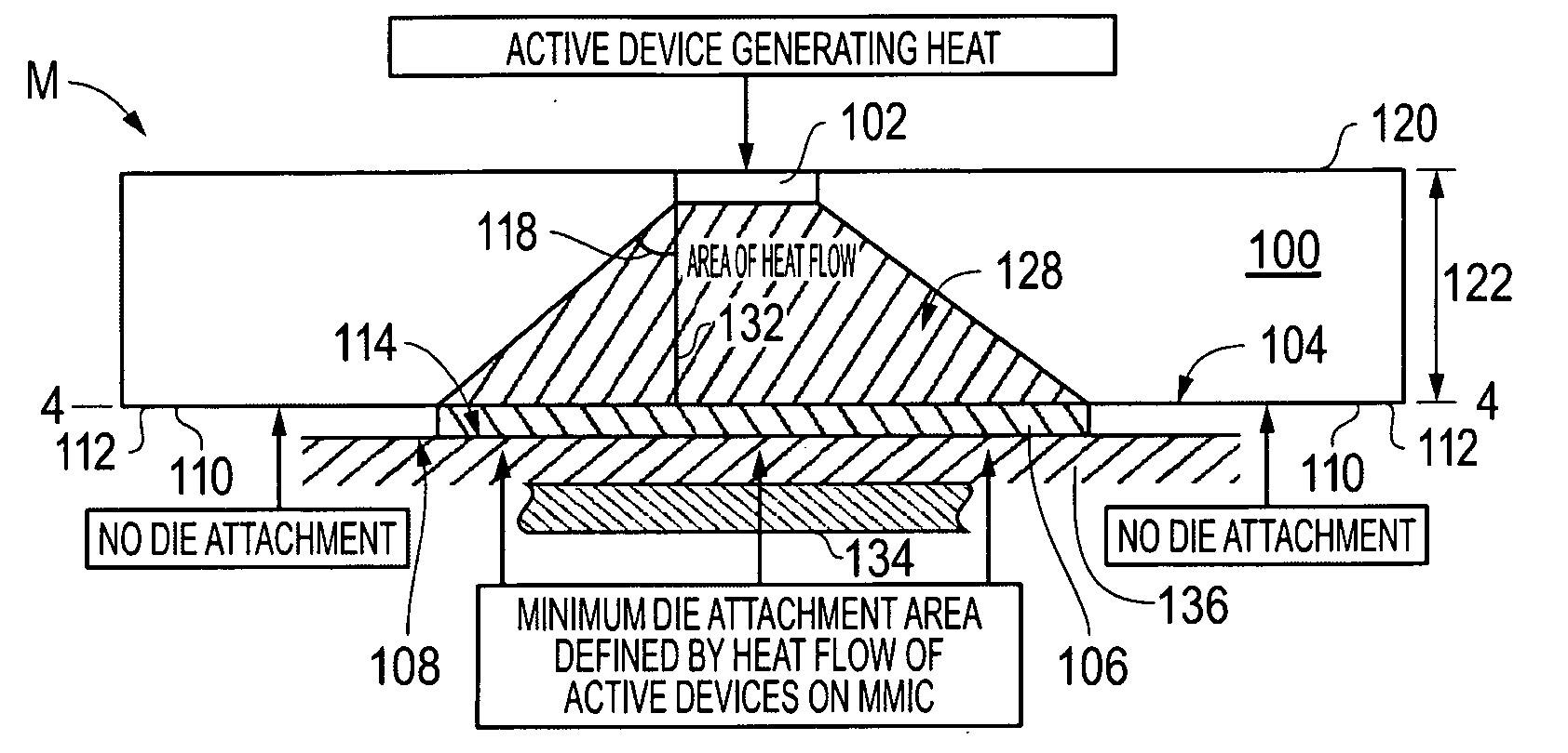
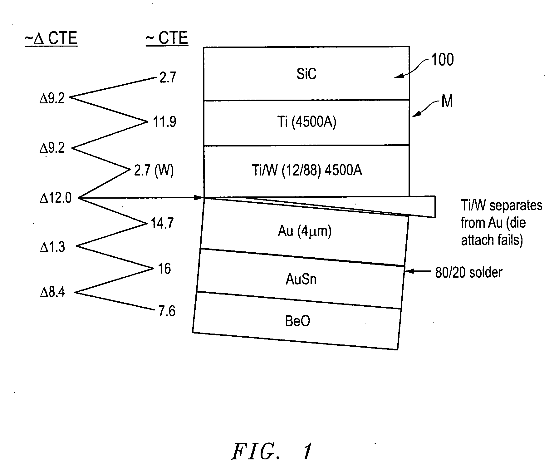
[0033]A semiconductor package M includes a semiconductor substrate layer 100 having a first side or upper surface 120 and a second side or lower surface or backplane 104 opposite the first side 120. A heat producing or active area 102 is formed associated with the first side 120 of the semiconductor substrate layer 100. A die attachment member 106 is formed in contact with the second side 104 of the semiconductor substrate layer 100 and extends over less than all of the second side 104 of the semiconductor substrate layer 100. The die attachment material 106 is essentially uniformly disposed opposite of...


PUM


Abstract

A semiconductor package (M) includes a semiconductor substrate layer (100) having a first side or upper surface (120) and a second side or lower surface or backplane (104) opposite the first side (120). A heat producing active area (102) is formed associated with the first side (120) of the semiconductor substrate layer (100). A die attachment member (106) is formed in contact with the second side (104) of the semiconductor substrate layer (100) and extends over less than all of the second side (104) of the semiconductor substrate layer (100). The die attachment material (106) is essentially uniformly disposed opposite of the heat producing area (102) with relation to the semiconductor substrate layer (100).

Description

CROSS REFERENCE TO RELATED APPLICATIONS[0001]This application claims the benefit of U.S. Provisional Application Ser. No. 61043087, filed Apr. 7, 2008, entitled RELIABILITY IMPROVEMENT IN A COMPOUND SEMICONDUCTOR MMIC.BACKGROUND OF THE INVENTION[0002]1. Technical Field[0003]The invention relates to the field of semiconductor devices, and more particularly to pulsed, high-powered discrete devices and monolithic microwave integrated circuits (MMICs).[0004]2. Background Art[0005]Thermo-mechanical metal fatigue in compound semiconductors (GaN, GaAs, and SiC, for example) has been found to occur in pulsed, high-powered discrete devices and monolithic microwave integrated circuits (MMICs) that are used in known active electronically steered arrays (AESAs). The pulsed operation of the compound semiconductor devices has been shown to result in thermo-mechanical fatigue and early, wear-out failure of several compound semiconductor device technologies. Often, systems applications require tens...

Claims


Application Information

Patent Timeline
IPC IPC(8): H01L23/34H01L21/50
CPCH01L23/34H01L24/32H01L24/29H01L2224/04026H01L2224/29144H01L2224/32014H01L2924/0105H01L2924/01077H01L2924/01079H01L2924/10158H01L2924/10272H01L2924/10329H01L2924/1033H01L2924/13055H01L2924/13091H01L2924/14H01L2924/1423H01L2924/19041H01L2924/19042H01L2924/19043H01L24/27H01L2924/014H01L2224/29101H01L2924/0001H01L2224/29111H01L2924/1305H01L2924/0132H01L2924/00H01L2924/01006H01L2924/01014H01L2924/01007H01L2924/01031H01L2924/01022H01L2924/01074H01L2924/01033H01L2224/29099
Inventor LEWIS, RANDALL D.CRAMER, HARLAN CARL
Owner NORTHROP GRUMMAN SYST CORP
Why Eureka
Try Eureka