Organic Light-Emitting Diode With Transparent Multilayer Electrode

a multi-layer electrode, light-emitting diode technology, applied in the direction of discharge tube/lamp details, discharge tube luminescnet screens, electric discharge lamps, etc., can solve the problems of ti, ta, particularly difficult to deposit in vacuum, cr) is liable to damage the underlying organic layer, liable to react with silver, etc., to prevent the degradation of the diode's performance

Active Publication Date: 2009-10-08
COMMISSARIAT A LENERGIE ATOMIQUE ET AUX ENERGIES ALTERNATIVES
View PDF15 Cites 6 Cited by
  • Summary
  • Abstract
  • Description
  • Claims
  • Application Information

AI Technical Summary

Benefits of technology

[0012]The object of the invention is to limit the reactions between the silver of the first metallic layer and the dielectric material to prevent degradation of the diode performances.
[0019]The reactions between the silver of the first metallic layer and the dielectric material of the absorption-limiting dielectric layer are limited due to the aluminum-based second metallic layer which performs a “buffer” function, advantageously preventing degradation of the diode's performances which would result from these reactions.

Problems solved by technology

Such metals (in particular Ti, Ta) are particularly difficult to deposit in a vacuum (high sublimation temperature: 1600° C. to 1700° C.)
, or (in particular Cr) are liable to damage the underlying organic layers.
It has however been observed that dielectric materials which are the most suitable for limiting absorption by an underlying metallic layer of silver were often liable to react with the silver.
The chemical reactions at the interface between the metallic layer of silver and the transparent top dielectric layer that covers it are however liable to degrade on the one hand the electric performances of the diode, since injection and transporting of charges will be degraded, and on the other hand the optic performances, since the resonant light extraction optic cavity is “out of tune”.

Method used


Image

  • Organic Light-Emitting Diode With Transparent Multilayer Electrode
  • Organic Light-Emitting Diode With Transparent Multilayer Electrode
  • Organic Light-Emitting Diode With Transparent Multilayer Electrode

Examples


Embodiment Construction

[0025]The invention will be better understood on reading the following description, given for non-restrictive example purposes only with reference to the appended drawings in which:

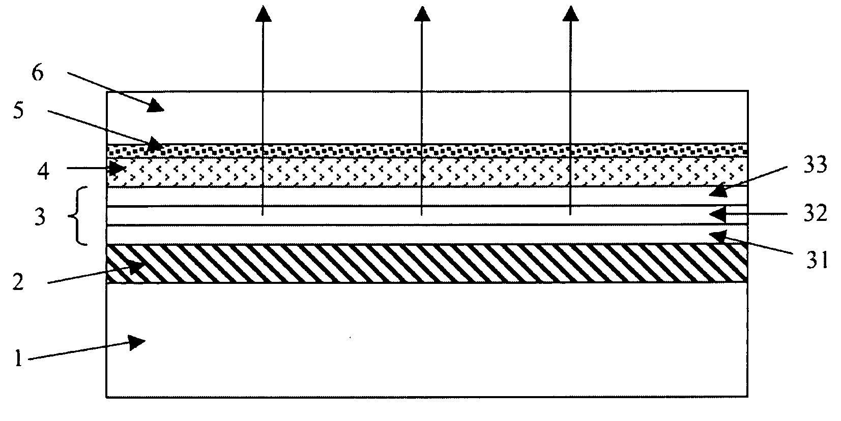
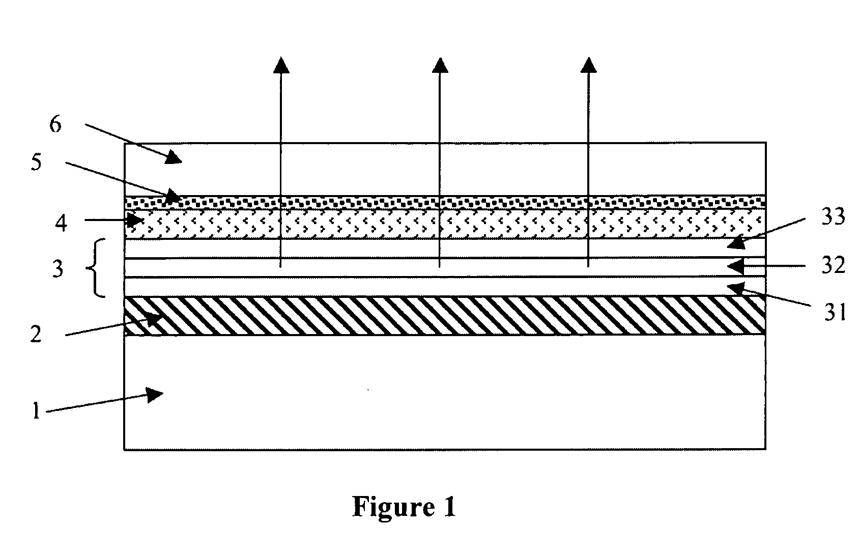
[0026]FIG. 1 illustrates a schematic view of a diode according to the invention, corresponding to a non-transparent substrate adapted to an “upward” photon emission, i.e. through the transparent top electrode;

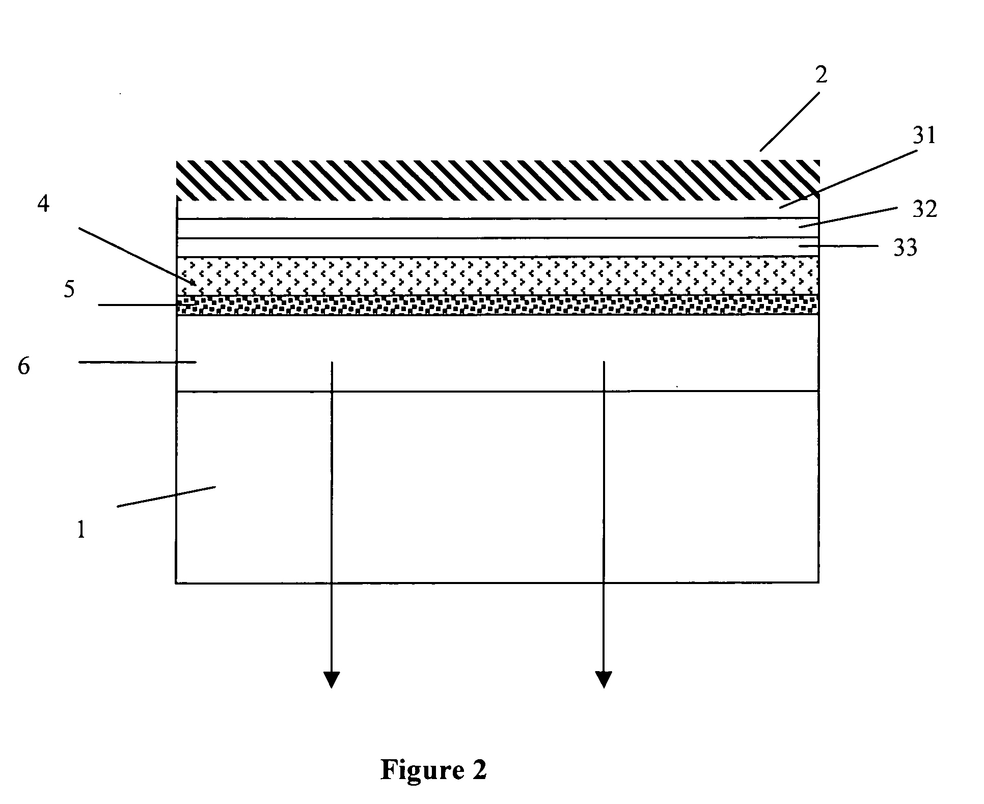
[0027]FIG. 2 is an alternative embodiment of FIG. 1 in which the substrate is transparent and adapted to a “downward” photon emission through the transparent bottom electrode which is in this case in direct contact with the substrate.

[0028]Fabrication of a diode according to the embodiment of FIG. 1 will now be described.

[0029]Bottom electrode 2, here an anode, is deposited on a substrate 1. It is formed by a metallic layer, for example made from silver, aluminum, or even gold, which are strongly reflecting metals. This electrode therefore forms here a reflecting bottom layer. The following are succe...


PUM

PropertyMeasurementUnit
total thicknessaaaaaaaaaa
thicknessaaaaaaaaaa

Abstract

An organic light-emitting diode comprising a substrate (1), an organic light-emitting layer (3) arranged between a first electrode (2) and a transparent and semi-reflecting second electrode with a multilayer structure subdivided into:a first silver-based metallic layer (4) in contact with the organic light-emitting layer (3),a second aluminum-based metallic layer (5),and a third dielectric layer (6),characterized in that the second metallic layer (5) is inserted between the first metallic layer (4) and the third dielectric layer (6) of the transparent second electrode, that the organic light-emitting layer (3) comprises a doped sub-layer in contact with the first metallic layer (4) of the transparent second electrode, and that the thickness of said third dielectric layer (6) is adjusted to limit the absorption by said first (4) and second (5) metallic layers of the light emitted by the diode.

Description

BACKGROUND OF THE INVENTION[0001]The invention relates to an organic light-emitting diode (OLED) with a transparent multilayer electrode, either bottom, in direct contact with the substrate, or top, opposite from the substrate with respect to the light-emitting layer.STATE OF THE ART[0002]In the document US 2005 / 0088080, a transparent electrode presents a multilayer structure in the following order: a LiF injection layer, an Ag layer, an Al layer, and a TeO2 dielectric.[0003]The document U.S. Pat. No. 5,969,474 describes an organic light-emitting diode comprising:[0004]an organic layer inserted between a bottom electrode in contact with a substrate and a transparent top electrode comprising a first metallic layer, for example made of silver alloy such as Mg—Ag, which is in contact with the organic layer,[0005]and a transparent top dielectric layer formed by a transparent conducting oxide such as ITO or IZO, which covers the first metallic layer.[0006]A buffer layer is inserted betwe...

Claims


Application Information

Patent Timeline
Patent Type & Authority Applications(United States)
IPC IPC(8): H01J1/63
CPCH01L51/5206H01L51/5265H01L51/5234H10K50/816H10K50/828H10K50/852
Inventor BETTINELLI, ARMANDMICHELLYS, JEAN-YVESMARTINEZ, JEAN-CLAUDE
Owner COMMISSARIAT A LENERGIE ATOMIQUE ET AUX ENERGIES ALTERNATIVES
Why Eureka
Try Eureka