Method and Its Apparatus for Inspecting Defects

a technology of defects and methods, applied in the direction of optically investigating flaws/contamination, optical radiation measurement, instruments, etc., can solve the problems of high sensitivity, patent documents 2 and 3 do not sufficiently take into account, and the inspection of defects on the edge portion is not taken into account, etc., to achieve high sensitivity and high speed

Inactive Publication Date: 2009-10-15
HITACHI HIGH-TECH CORP
View PDF3 Cites 25 Cited by
  • Summary
  • Abstract
  • Description
  • Claims
  • Application Information

AI Technical Summary

Benefits of technology

[0011]The present invention provides a method and apparatus for inspecting a minute defect present on the top and edge surfaces of a substrate such as a semiconductor substrate and a thin film substrate with high sensitivity and at high speed.
[0028]According to the present invention, the edge grip holding the sample has roughness (on the top and edge surfaces thereof) small enough to ensure that light scattered from the edge grip has a smaller intensity than that of light scattered from a defect present on the sample or that the light detectors are not saturated by light. In addition, the edge grip has a three-dimensional shape to prevent light diffracted from the edge grip from being incident on a main light detector.
[0029]According to the present invention, a portion of the sample, which is located near the edge portion of the sample, can be inspected with high sensitivity in a similar manner to inspection of a top surface of the sample.

Problems solved by technology

However, the defect inspection on the edge portion is not taken into account in Patent Document 1.
However, Patent Documents 2 and 3 do not sufficiently take into account the inspection of a substrate portion located near the edge portion of the substrate at high speed and with high sensitivity.

Method used


Image

  • Method and Its Apparatus for Inspecting Defects
  • Method and Its Apparatus for Inspecting Defects
  • Method and Its Apparatus for Inspecting Defects

Examples


Embodiment Construction

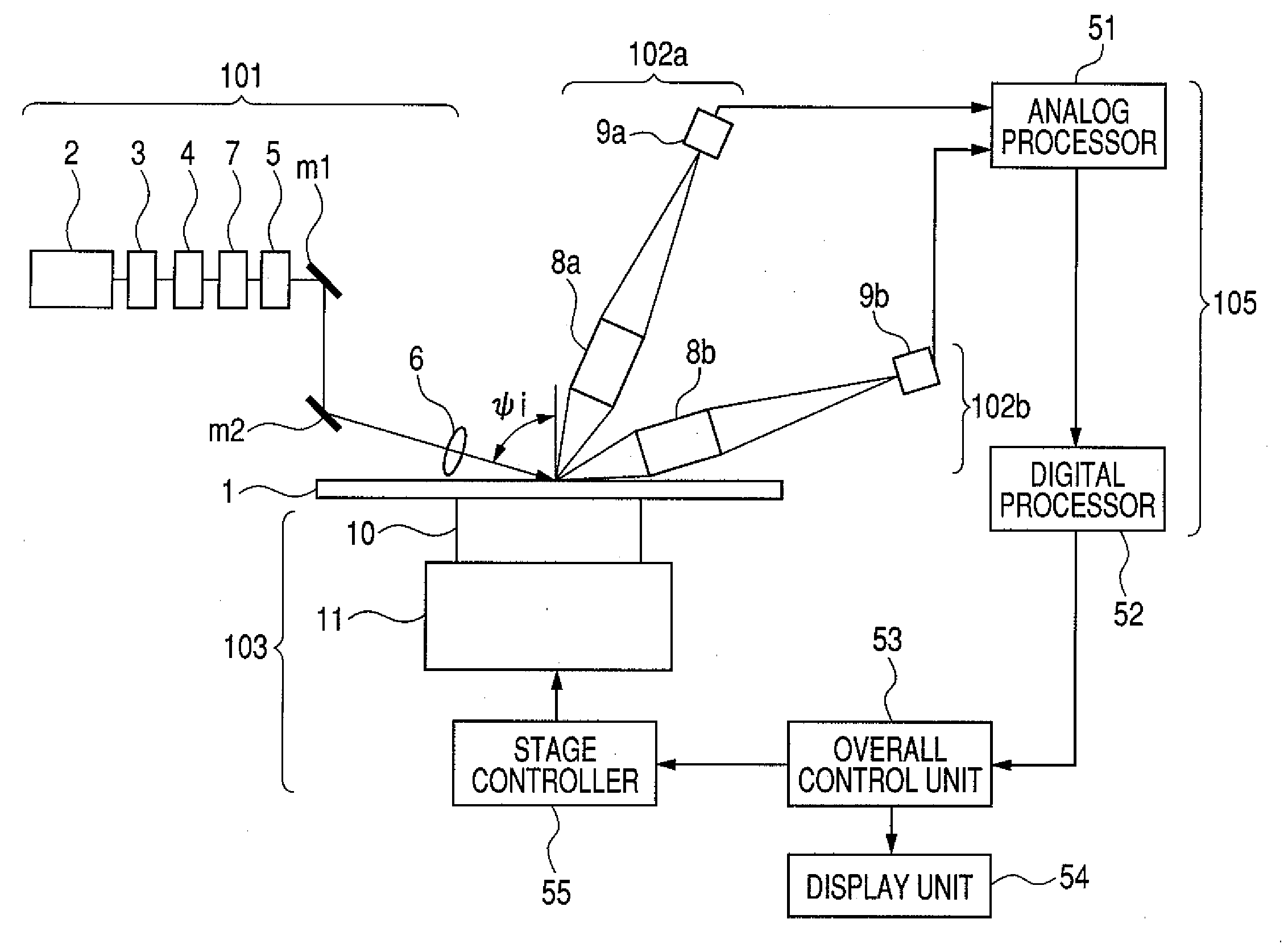
[0063]FIG. 1 illustrates the configuration of a defect inspection apparatus according to an embodiment of the present invention. The defect inspection apparatus includes an illumination optical system 101; detection optical units 102a and 102b; a stage 103 capable of mounting a wafer 1 thereon; a signal processor 105; an overall control unit 53; and a display unit 54.

[0064]The illumination optical system 101 includes a laser source 2, an attenuator 3, a polarizing element 4, a beam expander 7, an illumination intensity distribution control element 5, reflective mirrors m1 and m2, and a focusing lens 6. The laser source 2 emits a laser beam. The attenuator 3 adjusts the emitted laser beam to a given intensity. The polarizing element 4 then adjusts the intensity-adjusted laser beam to a polarized state desired. The beam expander 7 adjusts the resultant laser beam to a given beam diameter. The diameter-adjusted laser beam is then directed by the reflective mirrors and the focusing lens...


PUM

PropertyMeasurementUnit
elevation angleaaaaaaaaaa
sizeaaaaaaaaaa
areaaaaaaaaaaa

Abstract

A defect inspection apparatus is capable of inspecting an extremely small defect present on the top and edge surfaces of a sample such as a semiconductor substrate or a thin film substrate with high sensitivity and at high speed. The defect inspection apparatus has an illumination optical system, a plurality of detection optical units and a signal processor. One or more of the detection optical units receives either light diffracted from an edge portion of the sample or light diffracted from an edge grip holding the sample. The one or more of the detection optical units shields the diffracted light received by the detection optical unit based on a signal obtained by monitoring an intensity of the diffracted light received by the detection optical unit in order to inspect a sample portion located near the edge portion and a sample portion located near the edge grip.

Description

BACKGROUND OF THE INVENTION[0001]The present invention relates to a method and apparatus for inspecting a defect present on the top and edge surfaces of a sample such as a semiconductor substrate and a thin film substrate with high sensitivity and at high speed.[0002]In a production line for a semiconductor substrate or for a thin film substrate, an inspection operation is performed to inspect a defect on the surface of the semiconductor substrate or on the surface of the thin film substrate in order to maintain or improve the yield of products.[0003]As a conventional method and apparatus for inspecting a defect, JP-A-H09-304289 (Patent Document 1), JP-A-2003-240730 (Patent Document 2) and JP-A-2008-32621 (Patent Document 3) are known.[0004]Patent Document 1 discloses an apparatus for inspecting the surface of a wafer. The apparatus described in Patent Document 1 has a low-angle optical receiver and a high-angle optical receiver. The low-angle optical receiver is located such that i...

Claims


Application Information

Patent Timeline
Patent Type & Authority Applications(United States)
IPC IPC(8): G01J4/00G01N21/88
CPCG01N21/9503G01N21/9501
Inventor URANO, YUTANAKAO, TOSHIYUKIOSHIMA, YOSHIMASA
Owner HITACHI HIGH-TECH CORP
Why Eureka
Try Eureka