Electronic component module

a technology of electronic components and components, applied in the direction of final product manufacturing, sustainable manufacturing/processing, semiconductor/solid-state device details, etc., can solve the problems of limiting the amount of bonding strength and the limiting amount of shock resistance that can be improved, so as to improve the shock resistance and the effect of less likely to be damaged

Inactive Publication Date: 2009-10-22
MURATA MFG CO LTD
View PDF0 Cites 3 Cited by
  • Summary
  • Abstract
  • Description
  • Claims
  • Application Information

AI Technical Summary

Benefits of technology

[0008]To overcome the problems described above, preferred embodiments of the present invention provide an electronic component module that has further enhanced shock resistance and that is less likely to be damaged if bending or deformation is developed in the motherboard due to a shock, such as a drop.
[0010]In accordance with preferred embodiments of the present invention, no bonding material applying lands are present at the corner portions and the corner portion inner lands are provided. Thus, when mounted on a motherboard, no portions to which bonding material is applied are present at the corner portions. This removes stress concentration at the corner portions and prevents cracks or peeling from occurring. Thus, shock resistance is enhanced.

Problems solved by technology

However, there is a definite limit to how much the bonding strength can be improved only by changing the shapes of terminal electrodes as disclosed in the Patent Documents 1 to 3.
In other words, there has been a definite limit to how much the shock resistance can be improved using techniques in the known art that are directed to enhancing the bonding strength of the terminal electrodes at the four corners where stress tends to be concentrated.

Method used


Image

  • Electronic component module
  • Electronic component module
  • Electronic component module

Examples


first preferred embodiment

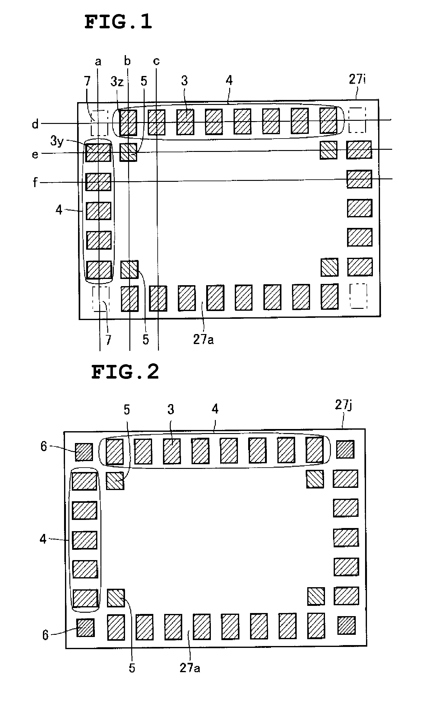
[0025]An electronic component module in a first preferred embodiment according to the present invention will be described with reference to FIG. 1. FIG. 1 shows the rear surface 27a of the electronic component module 27i, that is, the surface on which soldering lands are arranged. The electronic component module 27i is an electronic component module that is provided with a ceramic substrate and a plurality of soldering lands 3. The ceramic substrate has the rear surface 27a preferably having a substantially rectangular shape. The plurality of soldering lands 3 are arranged on the rear surface 27a. The plurality of soldering lands 3 include outer peripheral land rows 4. Each of the outer peripheral land rows 4 is arranged in a line along each side of the rear surface 27a with the exception of corner portions 7 of the rear surface 27a. The corner portions 7 are areas in which no lands are present. However, lands are arranged in the areas of the corner portions 7 according to the known...

second preferred embodiment

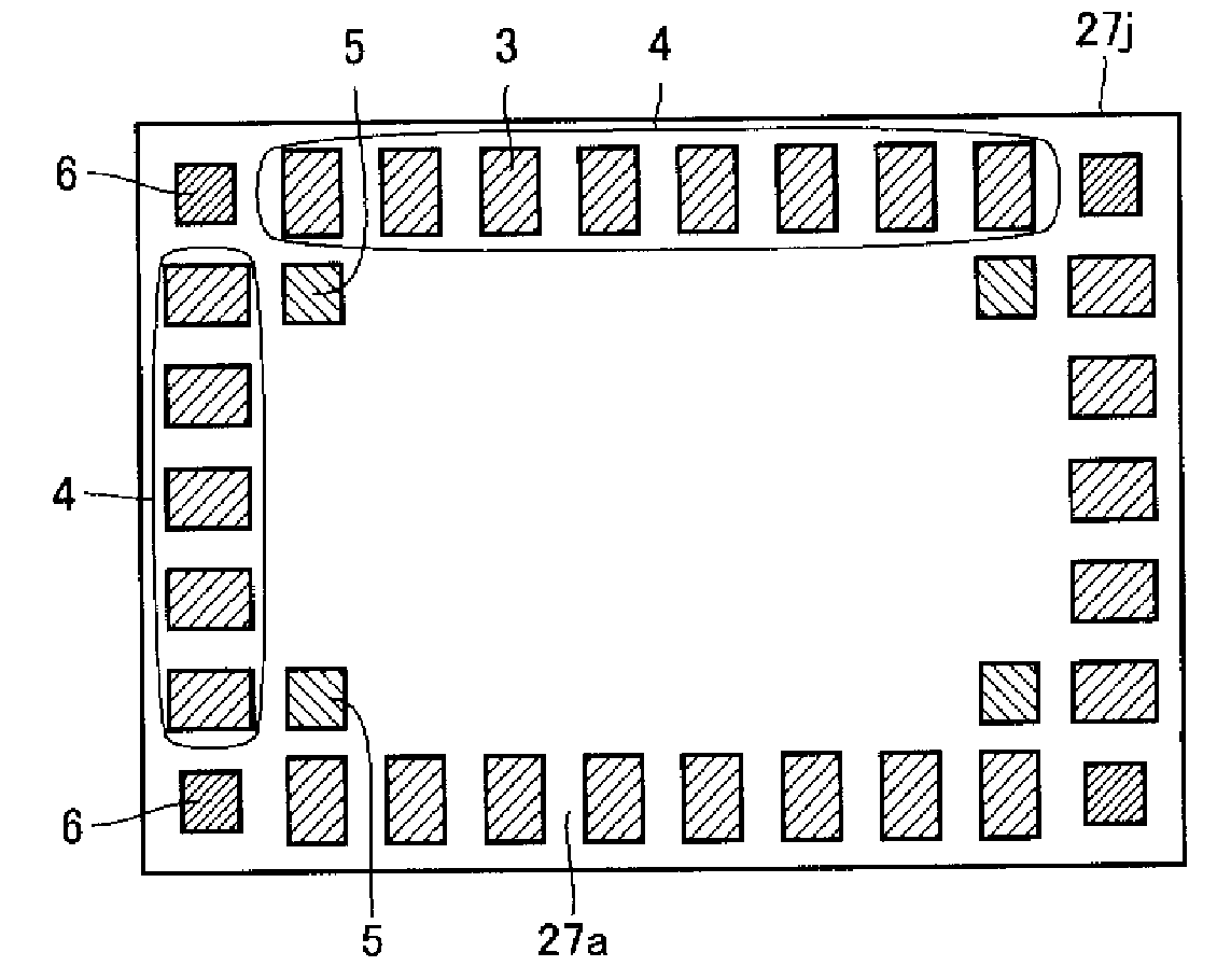
[0035]An electronic component module in a second preferred embodiment according to the present invention will be described with reference to FIG. 2. FIG. 2 shows the rear surface 27a of the electronic component module 27j. The electronic component module 27j is provided with the following structure in addition to the structure described in the first preferred embodiment. That is, non-soldering lands 6 are arranged at the corner portions of the rear surface 27a. The non-soldering lands 6 are lands that need not be soldered when the electronic component module 27j is mounted on the motherboard. For example, testing lands correspond to the non-soldering lands 6. The term “testing land” is a land that is electrically connected to a wiring pattern provided on the front surface or inside of the ceramic substrate for testing its electrical characteristics.

[0036]In this preferred embodiment, lands are arranged at the corner portions 7. However, the lands are not the soldering lands 3, and i...

third preferred embodiment

[0041]An electronic component module of a third preferred embodiment according to the present invention will be described with reference to FIG. 8. FIG. 8 shows the rear surface 27a of the electronic component module 27k. The electronic component module 27k is provided with the following structure in addition to the structure described in the first and second preferred embodiments. That is, the electronic component module 27k includes one or more short side inner land rows 8 that are arranged in lines along each short side of the substantially rectangular rear surface 27a and adjacent to the inner side of the outer peripheral land row 4.

[0042]In this preferred embodiment, because the bonding area may be increased between the electronic component module 27k and the motherboard, while avoiding stress concentration at the corner portions, shock resistance is enhanced.

[0043]The short side inner land row 8 may be arranged on only one of the short sides. However, it is preferable that the...


PUM


Abstract

An electronic component module is provided with a ceramic substrate and a plurality of bonding material applying lands. The ceramic substrate has a rear surface that is substantially rectangular. The plurality of bonding material applying lands are arranged on the rear surface. The plurality of bonding material applying lands includes outer peripheral land rows, each of which is arranged in a line along each side of the rear surface with the exception of corner portions of the rear surface. The plurality of bonding material applying lands includes corner portion inner lands, each of which is arranged on the rear surface at a location that is shifted inwardly in a substantially diagonal direction from the corner portion and is adjacent to the bonding material applying lands closest to the corner portion at ends of the outer peripheral land rows that are arranged in lines along two sides that are connected by the corner portion.

Description

BACKGROUND OF THE INVENTION[0001]1. Field of the Invention[0002]The present invention relates to an electronic component module, and more specifically, to an electronic component module that is provided with a ceramic substrate. In particular, the present invention relates to a high-frequency module that includes a number of terminal electrodes arranged on the rear surface.[0003]2. Description of the Related Art[0004]A high-frequency module is an example of an electronic component module that is provided with a ceramic substrate. A high-frequency module that integrates devices having various functions, such as switches, filters, couplers, baluns and amplifiers, is used for wireless devices, such as mobile communication devices and wireless LANs. The high-frequency module is configured so that surface mounting components, such as semiconductor devices and ceramic capacitors, which define functional devices, are mounted on the front surface of a ceramic multilayer substrate, wherein w...

Claims


Application Information

Patent Timeline
Patent Type & Authority Applications(United States)
IPC IPC(8): H05K1/00
CPCH01L23/15H01L23/49816H01L23/49838H01L2224/16225H05K2201/10727H05K3/3442H05K2201/094H05K2201/09409H01L2924/09701H01L2224/81385Y02P70/50H01L25/04
Inventor SUESADA, TSUYOSHIHIGASHIBATA, KAZUAKIHOSOKAWA, TOSHIHIROKAWATA, MASAKI
Owner MURATA MFG CO LTD
Why Eureka
Try Eureka