Conductive laminate and touch panel using same
a technology of conductive laminate and touch panel, which is applied in the direction of conductive layers on insulating supports, pulse techniques, instruments, etc., can solve the problems of considerable durability decline, risk of damage, and wetness, and achieve the effect of favorable visibility
- Summary
- Abstract
- Description
- Claims
- Application Information
AI Technical Summary
Benefits of technology
Problems solved by technology
Method used
Image
Examples
example 1
Production of Conductive Film
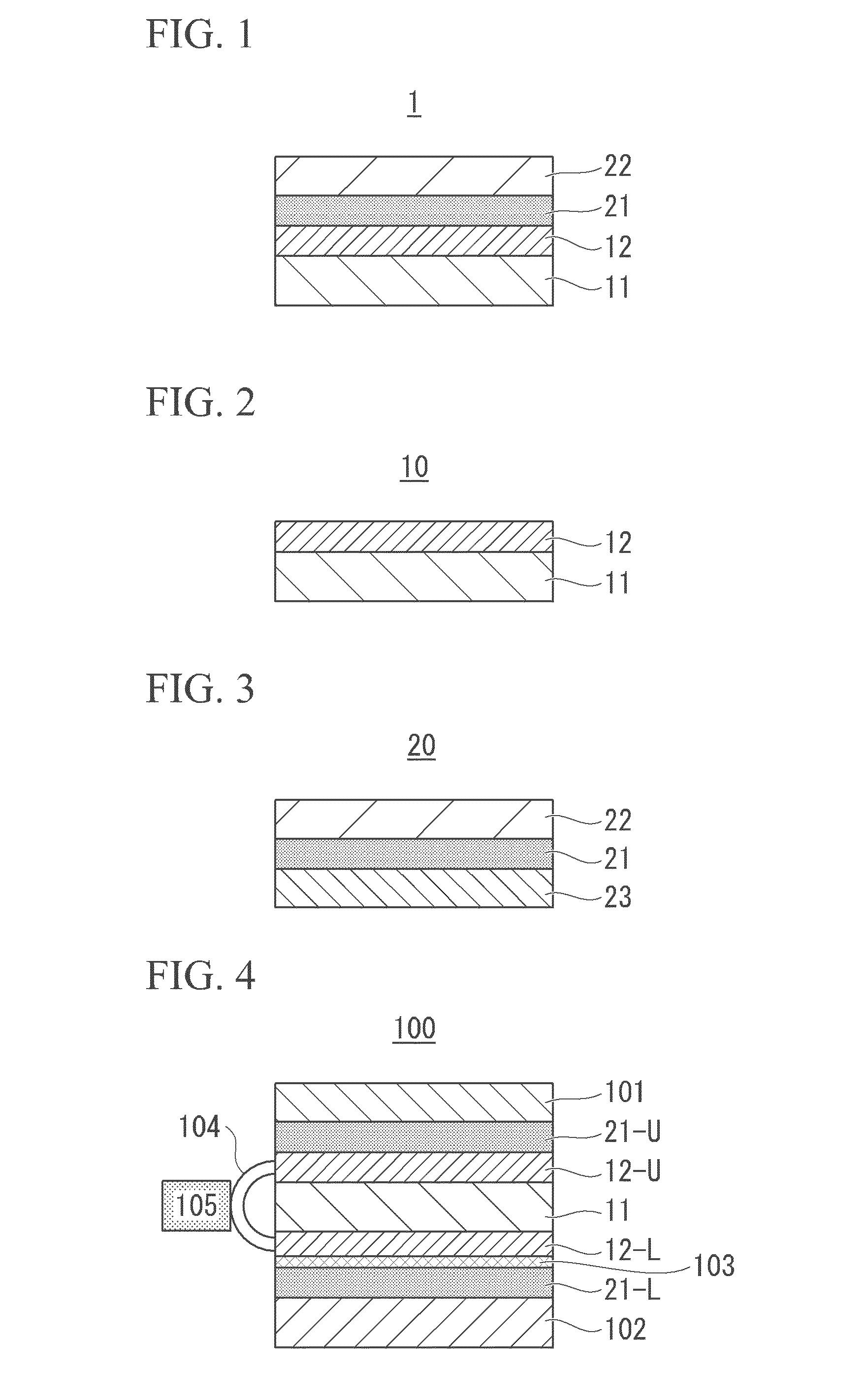
[0118]An aqueous dispersion containing a conductive substance obtained by polymerizing 3,4-ethylenedioxythiophene in the presence of polystyrene sulfonate (abbreviated as PEDOT-PSS) was mixed with a binder component in the form polyester resin (Vylonal MD1200, Toyobo Co., Ltd.) and a fluorine-based surfactant (Megafac F-556, DIC Corp.) at a ratio of 1:1:1 as the solid fraction, followed by diluting with methanol to obtain a mixture A having a solid concentration of 1%. This dispersion was then mixed with a 1% solution of a silane coupling agent (KBM-403, Shin-Etsu Silicone Co., Ltd.), obtained by diluting with a 50 / 50 mixture of water and methanol, at a weight ratio of 100:30 to prepare a conductive coating agent A. This conductive coating agent A was coated onto one side of a first base material in the form of a biaxially oriented polyethylene terephthalate film provided with a surface-treated highly adhesive layer on both sides thereof (trade name: Cos...
example 2
[0132]A double-sided conductive film 2 having a total luminous transmittance of 88.6% was produced by adjusting the thickness of the conductive layer so as to obtain surface resistivity of 287 Ω / sq in the same manner as Example 1 with the exception of using a silicone-based surfactant (Leveling Agent KP-110, Shin-Etsu Silicone Co., Ltd.) as a conductive coating agent B instead of the fluorine-based surfactant, and a conductive laminate 2 and a liquid crystal module 2 provided with a touch panel were produced using this double-sided conductive film 2.
example 3
[0133]A double-sided conductive film 3 having a total luminous transmittance of 88.0% was produced by adjusting the thickness of the conductive layer so as to obtain surface resistivity of 287 Ω / sq in the same manner as Example 2 with the exception of mixing a mixture B, a 1% solution obtained by diluting a silane coupling agent (KBM-403, Shin-Etsu Silicone Co., Ltd.) with methanol, and a 1% solution obtained by diluting a melamine-based crosslinking agent (Sumimarl M-50W, Sumitomo Chemical Co., Ltd.) with methanol, at ratio of 100:15:15 for use as a conductive coating agent C, and a conductive laminate 3 and a liquid crystal module 3 provided with a touch panel were produced using this double-sided conductive film 3.
PUM
| Property | Measurement | Unit |
|---|---|---|
| contact angle | aaaaa | aaaaa |
| luminous transmittance | aaaaa | aaaaa |
| luminous transmittance | aaaaa | aaaaa |
Abstract
Description
Claims
Application Information


