Interconnection system on a plane adjacent to a solid-state device structure

a solid-state device and interconnection system technology, applied in the direction of microstructural devices, electrical transducers, instruments, etc., can solve the problems of complex three-dimensional structures with components that are difficult to interconnect, complex crossover structures, and inability to multi-planar interconnect systems within the device substrate. achieve the effect of keeping the total surface small and reducing the amount of surface area

Active Publication Date: 2009-10-22
PCB PIEZOTRONICS OF NORTH CAROLINA
View PDF7 Cites 5 Cited by
  • Summary
  • Abstract
  • Description
  • Claims
  • Application Information

AI Technical Summary

Benefits of technology

[0011]A further object of the present invention is to provide an interconnection system for a MEMS device that minimizes the amount of surface on a sensor wafer used for wiring, to keep the total surface small.

Problems solved by technology

MEMS fabrication techniques, such as deep reactive ion etching (DRIE) can produce complex three dimensional structures with components that are difficult to interconnect.
MEMS devices may include regions that are completely etched through from a top surface to a bottom surface of a semiconductor wafer, such that a conventional via-connected, multi-planar interconnect system within a device substrate is not feasible.
For example, a conventional, full-bridge accelerometer with cantilevered seismic masses and strain gauges can be fabricated as a MEMS structure, but the electrical connection of the bridge requires complicated crossover structures or very delicate wire-bonding on a device that may be on the order of 1 millimeter across.
The interconnection problem may be exacerbated when multiple devices are fabricated on a single MEMS substrate, such as a tri-axial accelerometer, for example, where several crossover structures may be required and multiple wire bonds must be made to the MEMS device and to contacts that provide external access to the MEMS device, such as a lead frame.
Additionally, wire bonds may reduce the reliability of a MEMS device in harsh temperature, shock and vibration environments such as automotive and military applications.

Method used


Image

  • Interconnection system on a plane adjacent to a solid-state device structure
  • Interconnection system on a plane adjacent to a solid-state device structure
  • Interconnection system on a plane adjacent to a solid-state device structure

Examples


Embodiment Construction

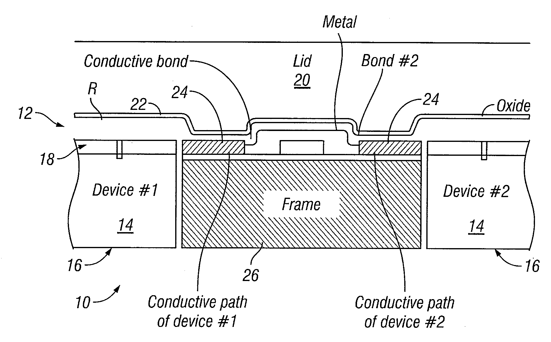
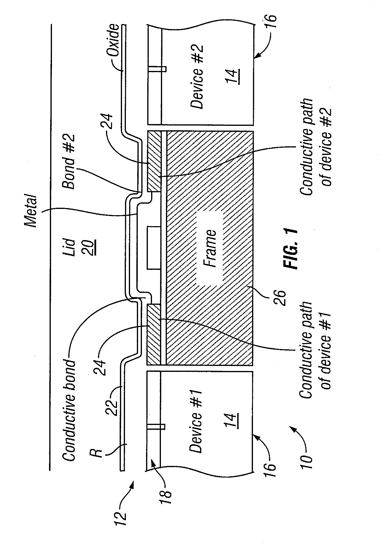
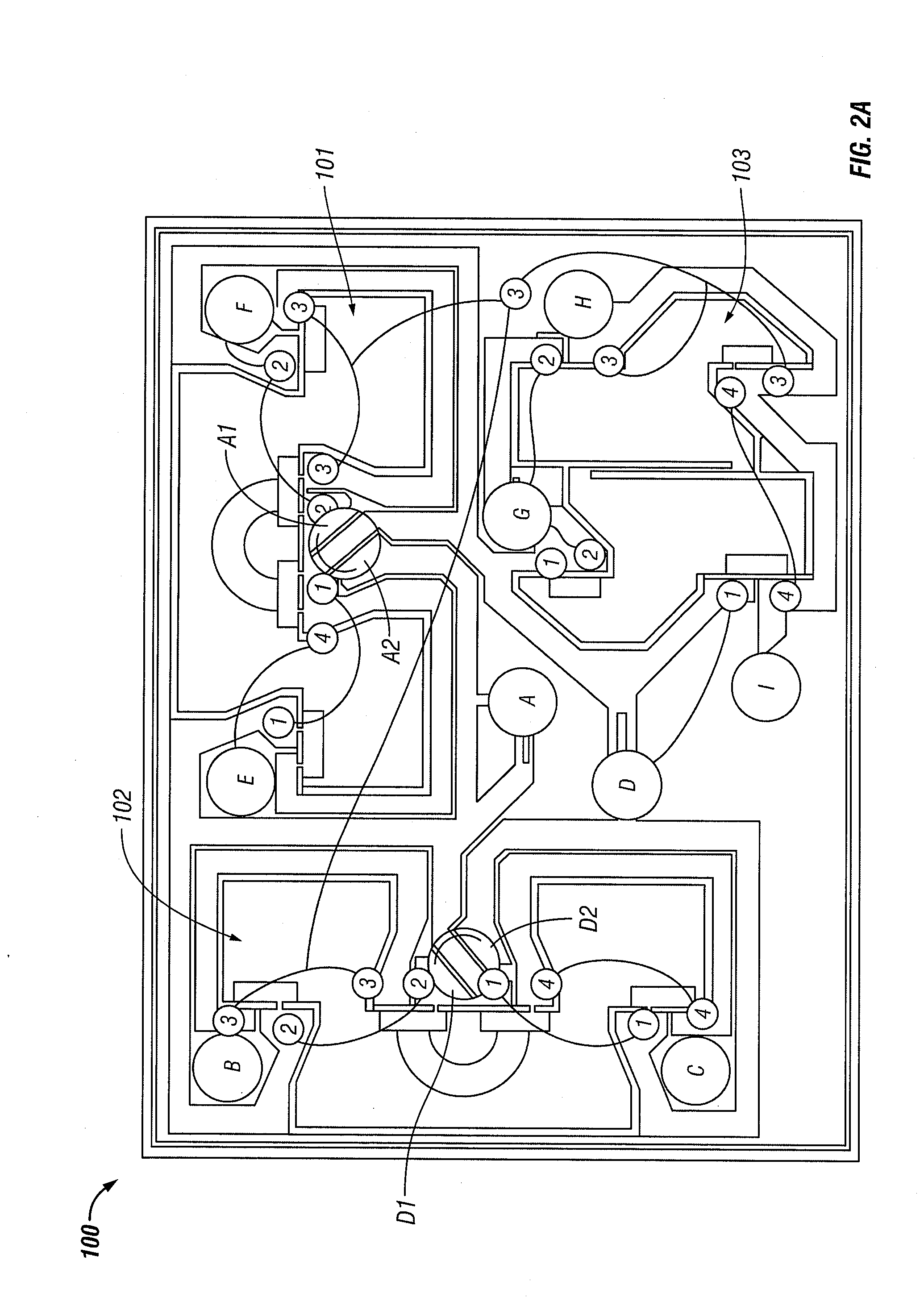
[0030]In one embodiment of the present invention, an interconnection system is provided for solid-state devices. Solid-state devices include but not limited to, accelerometers, pressure sensors, resonators and relays. The accelerometer can be, (i) single axis, linear, (ii) single axis, rotational, (iii) two-axis, (iv) three axis, (v) x-axis, rotational and linear, (vi) piezoresistive and (vii) variable capacitance. The interconnection system can be for any type of semiconductor device or semiconductor technology requiring interconnections that cannot be achieved in a single plane or interconnections that cannot be achieved using conventional vias and multiple interconnection planes within a single multilayer substrate. The advantage of the present invention is that much of a formerly little-use surface becomes available for use as a printed-wire board.

[0031]The present invention is applicable to any device in which two or more wafers are bonded together, and is particularly applicab...


PUM


Abstract

An interconnection system is provided for a solid-state device. The solid-state that includes, a first layer, multiple devices and a first face. A second layer is bonded to the first face at a bonded face of the second layer that faces the first face. Electrically conductive bonds are between the first and second faces. Conductive paths are on the bonded face of the second layer and connect two or more of the conductive bonds.

Description

CROSS-REFERENCE TO RELATED APPLICATIONS[0001]This application claims the benefit of U.S. Ser. No. 61 / 039,646, filed Mar. 26, 2008, which application is fully incorporated herein by reference.BACKGROUND OF THE INVENTION[0002]1. Field of the Invention[0003]This invention relates generally to interconnection systems and, in particular, to interconnection systems for solid-state devices.[0004]2. Description of the Related Art[0005]Microelectromechanical systems (MEMS) often include integrated electrical and mechanical components that require, respectively, electrical interconnections and mechanical couplings. MEMS fabrication techniques, such as deep reactive ion etching (DRIE) can produce complex three dimensional structures with components that are difficult to interconnect. MEMS devices may include regions that are completely etched through from a top surface to a bottom surface of a semiconductor wafer, such that a conventional via-connected, multi-planar interconnect system within ...

Claims


Application Information

Patent Timeline
Patent Type & Authority Applications(United States)
IPC IPC(8): H01L29/84H01L23/535
CPCB81B7/0006B81B2201/0235B81B2207/07B81C1/00238G01P15/0802H01L2924/0002G01P15/123H01L2924/00
Inventor WILNER, LESLIE BRUCE
Owner PCB PIEZOTRONICS OF NORTH CAROLINA
Why Eureka
Try Eureka