Trenched substrate for crystal growth and wafer bonding

a technology of crystal growth and substrate, applied in the direction of crystal growth process, chemically reactive gas, chemistry apparatus and processes, etc., can solve the problems of undesired cost of wafer rejection and the entire wafer being rejected, so as to reduce the likelihood, mitigate the stress build up within the substrate, and mitigate the effect of stress

Inactive Publication Date: 2009-10-29
KK TOSHIBA
View PDF61 Cites 33 Cited by
  • Summary
  • Abstract
  • Description
  • Claims
  • Application Information

AI Technical Summary

Benefits of technology

[0006]More particularly, in accordance with an example of an embodiment a substrate for an LED can comprise at least one trench formed therein so as to mitigate stress build up within the substrate. Any desired number of such trenches can be formed in any desired pattern and/or configuration.
[0007]In accordance with an example of an embodiment, a method for making LEDs can comprise forming at least one trench in a substrate so as to mitigate stress build up within the substrate. Any desired number of

Problems solved by technology

As those skilled in the art will appreciate, such damage can result in the rej

Method used


Image

  • Trenched substrate for crystal growth and wafer bonding
  • Trenched substrate for crystal growth and wafer bonding
  • Trenched substrate for crystal growth and wafer bonding

Examples


Embodiment Construction

[0022]Systems and methods are disclosed herein to provide substrates, such as sapphire wafers, for use in light emitting diode (LED) fabrication and the like. The wafers can be substantially less susceptible to damage during the fabrication process. For example, the wafers can be substantially less susceptible to damage caused by temperature change during such as the chemical vapor deposition (CVD) and wafer bonding process.

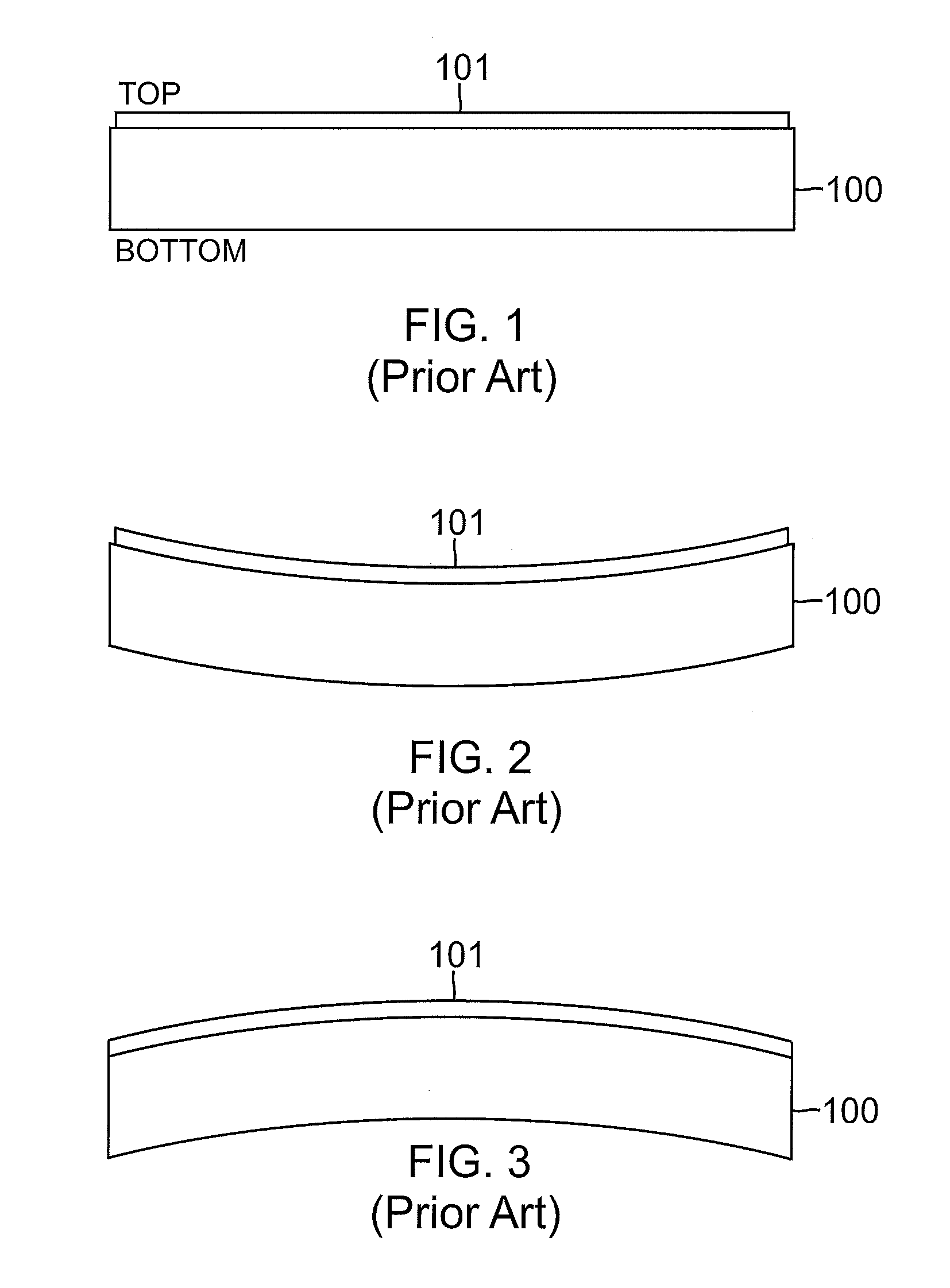
[0023]As discussed above, changes in temperature such as those that occur during the chemical vapor deposition process can cause a wafer to deform, crack, or even break apart. When this occurs, the wafer must generally be discarded. Further, it may be necessary to clean debris from the chemical vapor deposition chamber after such an incident.

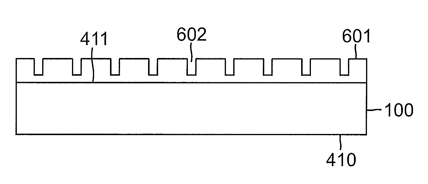
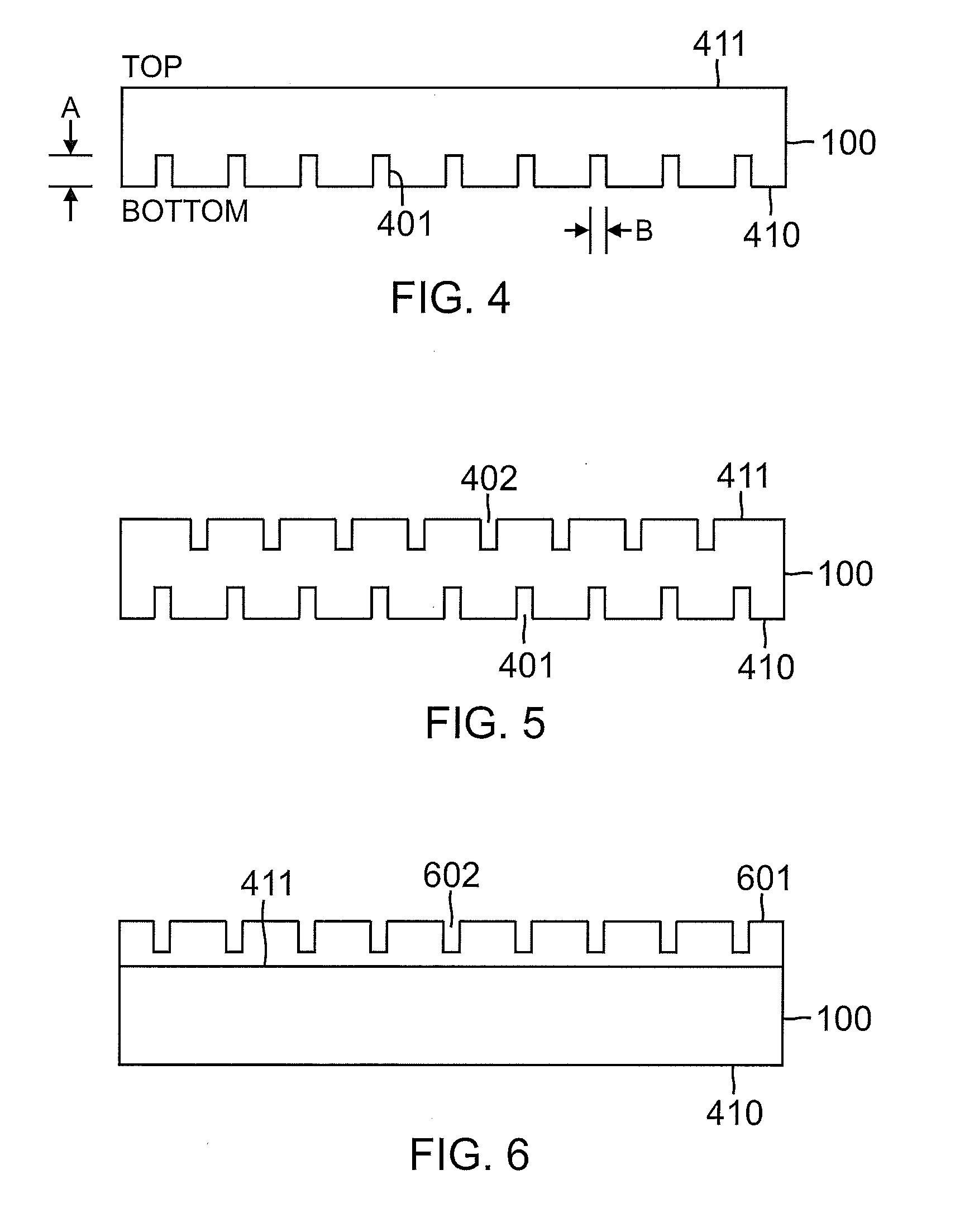
[0024]According to an example of an embodiment, a substrate for an LED can comprise one or more trenches formed therein so as to mitigate stress build up within the substrate. Any desired number of trenches and configuration ...


PUM


Abstract

A substrate for a light emitting diode (LED) can have one or more trenches formed therein so as to mitigate stress build up within the substrate due to mismatched thermal coefficients of expansion between the substrate and layers of material, e.g., semiconductor material, formed thereon. In this manner, the likelihood of damage to the substrate, such as cracking thereof, is substantially mitigated.

Description

TECHNICAL FIELD[0001]The present invention relates generally to the fabrication of devices such as light emitting diodes (LEDs). The present invention relates more particularly to the use of a substrate having trenches or the like formed therein so as to mitigate stress in the substrate during the fabrication of LEDs and other devices.BACKGROUND[0002]The use of substrates, such as those comprised of sapphire, Si, SiC, and ZnO in the fabrication of light emitting diodes (LEDs) is well known. Substrates are generally provided in the form of wafers. A single wafer can define substrates for many, e.g., hundreds or thousands, of LEDs. Layer of materials, such as semiconductors, conductors, and non-conductors, are formed upon such wafers to define the LEDs.[0003]A problem encountered in the contemporary fabrication of LEDs is the undesirable build up of stress in the wafers or substrates, as well as in materials formed upon the wafer or substrate. Such stress can result in deformation, cr...

Claims


Application Information

Patent Timeline
IPC IPC(8): H01L33/00H01L23/00
CPCC30B25/18H01L33/007H01L21/0243H01L21/0242
Inventor CUI, JIE
Owner KK TOSHIBA
Why Eureka
Try Eureka