

Functional Device and Method for Making the Same
- Summary
- Abstract
- Description
- Claims
- Application Information
AI Technical Summary
Benefits of technology
Problems solved by technology
Method used
Image

Examples
first embodiment
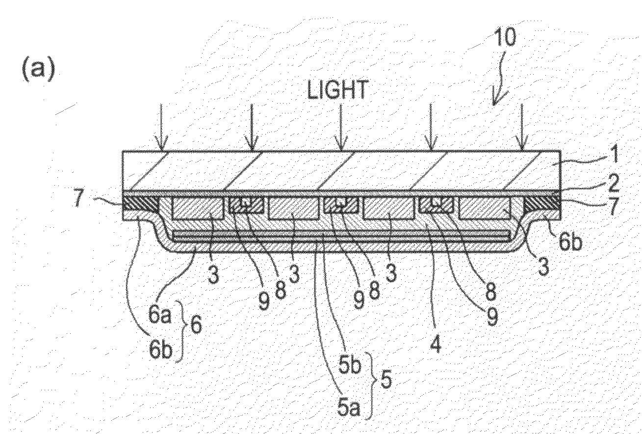
[0044]FIG. 1 includes a cross-sectional view (a) and a plan view (b) showing the structure of a dye-sensitized photovoltaic device 10 according to a first embodiment. Note that the cross-sectional view (a) is a cross-sectional view taken at the position shown by line 1A-1A in the plan view (b). In the plan view (b), only components formed on a transparent substrate 1 are depicted for easy recognition, and the position of a joint 11 between a film-shaped packaging member 6 and the transparent substrate 1 is surrounded and marked by dotted lines.
[0045]The dye-sensitized photovoltaic device 10 mainly corresponds to claim 1 and claim 2, and is constituted by the transparent substrate 1 formed of glass or the like, a transparent conductive layer 2 formed of FTO (fluorine-doped tin(IV) oxide, SnO2) or the like, semiconductor electrode layers 3 (negative electrodes) supporting a photosensitizing dye, an electrolyte layer 4, a film-shaped counter electrode (positive electrode) 5, a film-sha...
second embodiment
[0089]FIG. 3 includes a cross-sectional view (a) and a plan view (b) showing the structure of a dye-sensitized photovoltaic device 20 according to a second embodiment. Note that the cross-sectional view (a) is a cross-sectional view taken at the position shown by line 2A-2A in the plan view (b). In the plan view (b), only components formed on a transparent substrate 1 are depicted for easy recognition, and the position of a joint 24 of a film-shaped packaging member 21, the transparent substrate 1, and an light-incident-side film-shaped packaging member 22 is surrounded and marked by dotted lines.
[0090]The dye-sensitized photovoltaic device 20 mainly corresponds to claim 1 and claim 5, and is constituted by a transparent substrate 1 formed of glass or the like, a transparent conductive layer 2 formed of FTO (fluorine-doped tin(IV) oxide, SnO2) or the like, semiconductor electrode layers 3 (negative electrodes) supporting a photosensitizing dye, an electrolyte layer 4, a film-shaped ...
example 1
[0101]The dye-sensitized photovoltaic device 10 shown in FIG. 1 was prepared. A FTO layer as the transparent conductive layer 2 was formed on a transparent substrate 1, 32 mm×49 mm in size and 1.1 mm in thickness. As a titanium oxide, TiO2, paste, i.e., the material for forming the semiconductor electrode layer 3, Ti-Nanoxide TSP produced by Solaronix was used. This TiO2 paste was coated on the transparent conductive layer 2 by a screen printing method using a 150-mesh screen so as to form four semiconductor fine particle paste layers of stripe (strip) forms each 5 mm×40 mm in size. Subsequently, a silver fine particle layer 0.5 mm in width and 46 mm in length for forming the power-collecting wiring 8 was formed by a printing method on the transparent conductive layer 2 between the semiconductor fine particle paste layers.
[0102]Then TiO2 fine particles and the silver fine particles were sintered on the transparent conductive layer 2 composed of FTO by retaining at 500° C. for 30 min...
PUM
 Abstract
Description
Claims
Application Information