Imprint Method and Imprint Apparatus

a technology which is applied in the field of imprinting method and imprinting apparatus, can solve the problems of reducing size and increasing the cost of associated apparatuses, and achieve the effect of preventing accurate positioning of molds at the proper place and accurately reproducing pattern shapes

Inactive Publication Date: 2009-11-05
PIONEER CORP
View PDF4 Cites 26 Cited by
  • Summary
  • Abstract
  • Description
  • Claims
  • Application Information

AI Technical Summary

Benefits of technology

[0007]The conventional imprint technique, however, employs a fine pattern formed on a mold, so that thermal expansion and contraction of the mold due to temperature changes during the process causes a displacement of the mold from the substrate to make it impossible to accurately replicate the pattern shape. Since the substrate and the mold are cooled during the hardening of the transfer layer on the substrate with the transfer layer on the substrate ke

Problems solved by technology

As semiconductor devices are increasingly reduced in size, a photolithography technique suffers from an increased cost of associ

Method used


Image

  • Imprint Method and Imprint Apparatus
  • Imprint Method and Imprint Apparatus
  • Imprint Method and Imprint Apparatus

Examples


embodiment 1

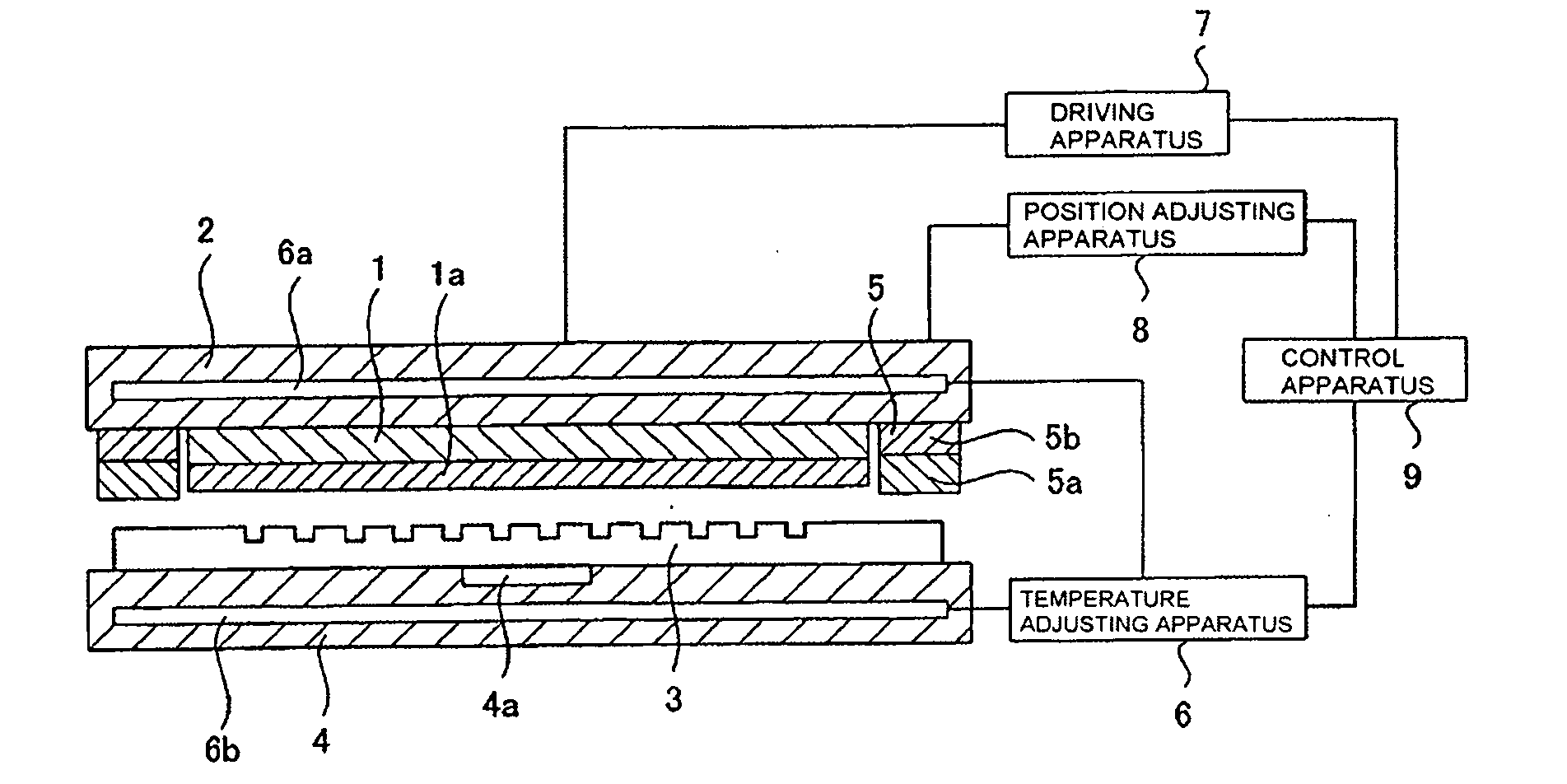
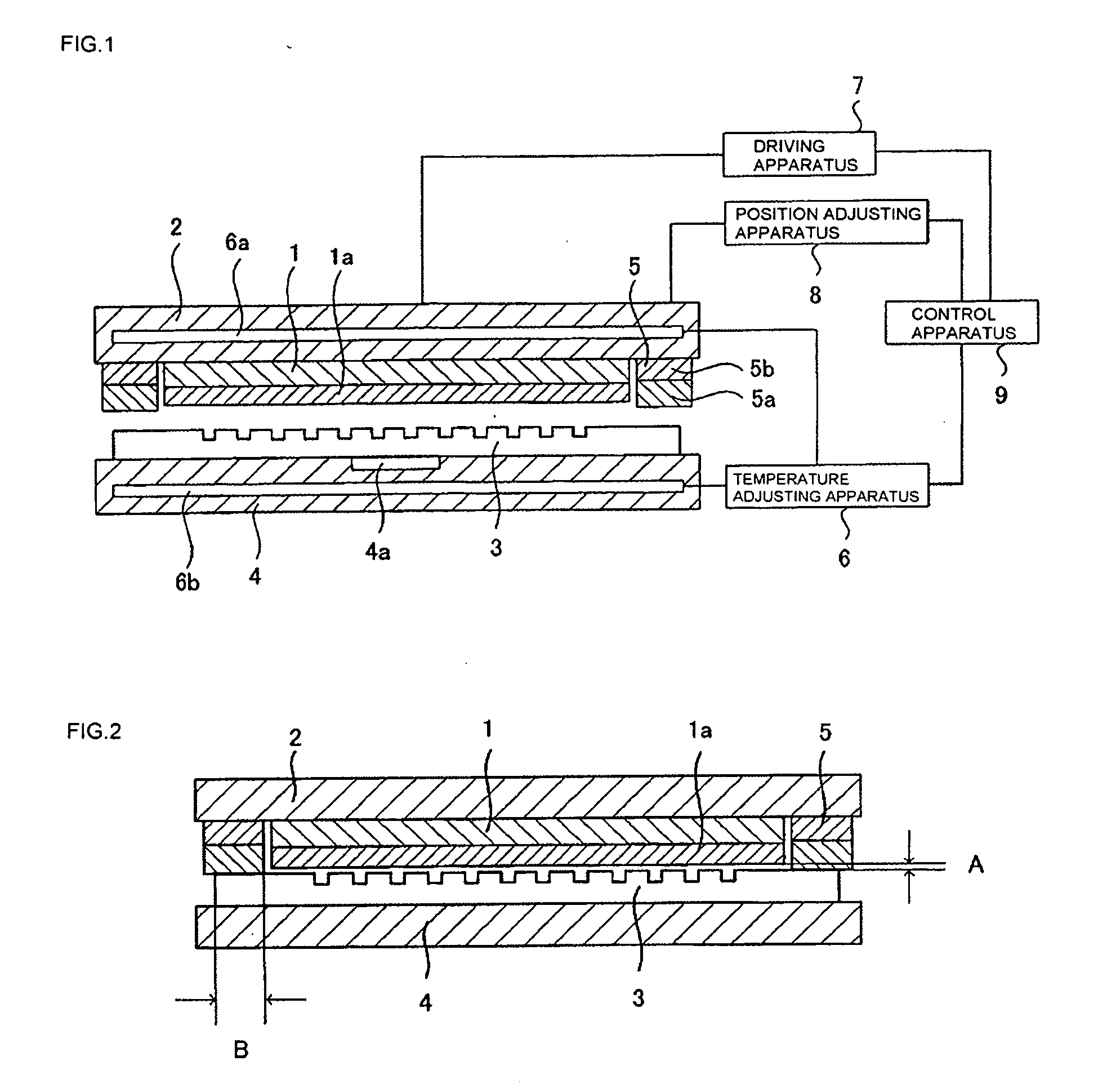
[0056]Embodiment 1 will be described with reference to FIGS. 1 to 6.

[0057]FIG. 1 is a schematic diagram showing an imprint apparatus of Embodiment 1 in cross section.

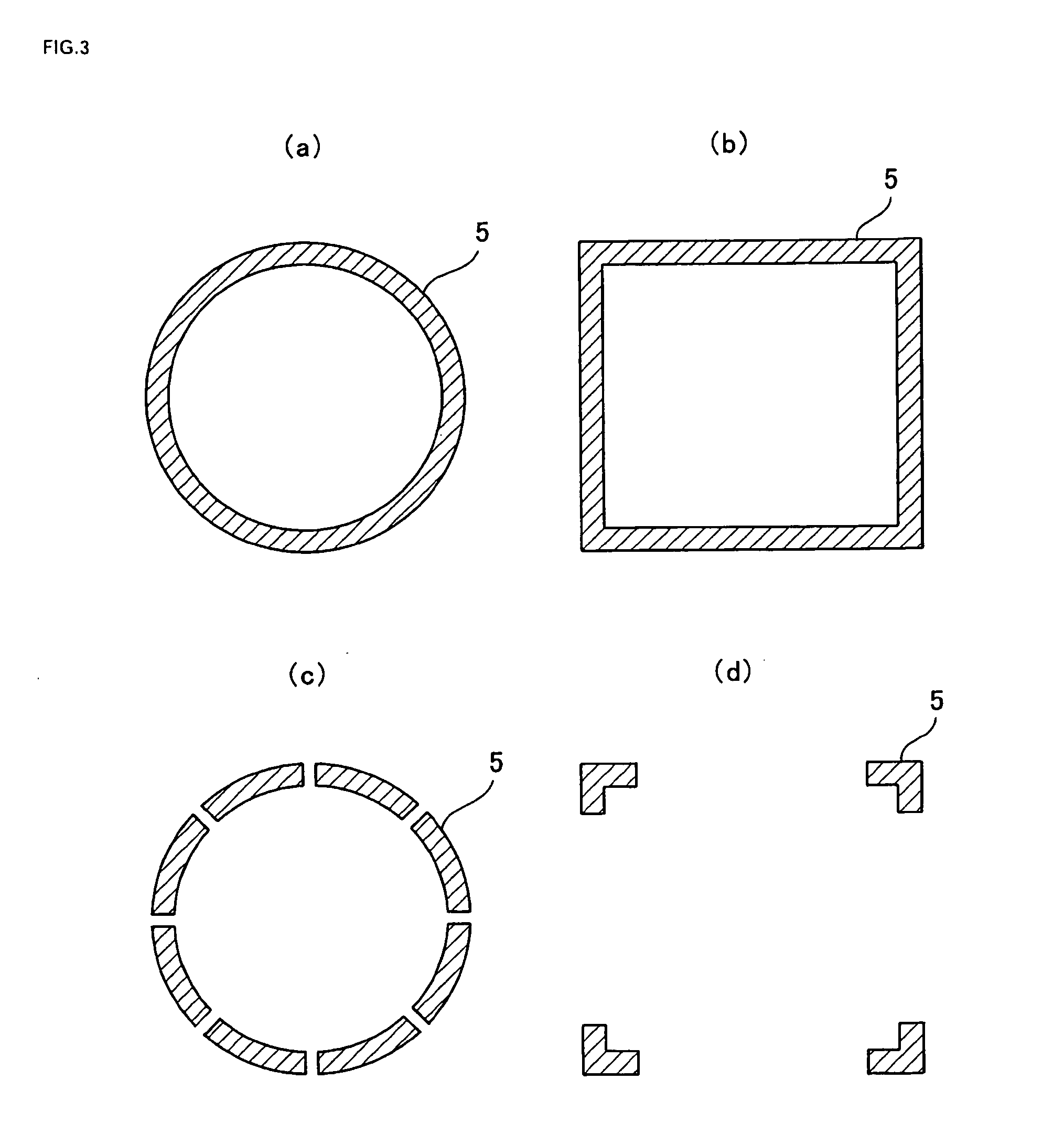
[0058]The imprint apparatus shown in FIG. 1 includes a substrate holding component 2 for holding a substrate 1 having a transfer layer 1a formed thereon, a mold holding component 4 for holding a mold 3 having a pattern formed thereon, a retaining component 5 for retaining a peripheral portion of a surface of the mold 3, a temperature adjusting apparatus 6 for adjusting the temperatures of the substrate 1 and the mold 3, a driving apparatus 7 for driving the substrate holding component 2 toward or away from the mold holding component 4 (in a vertical direction in FIG. 1), a position adjusting apparatus 8 for adjusting the relative positions of the substrate holding component 2 and the mold holding component 4, and a control apparatus 9 for controlling these apparatuses.

[0059]The substrate 1 can be a Si (silicon) substrat...

embodiment 2

[0112]Embodiment 2 will hereinafter be described with reference to FIG. 7. Components identical to those of Embodiment 1 described above are designated with the same reference numerals and description of the same component is omitted.

[0113]FIG. 7 is a schematic diagram showing an imprint apparatus according to Embodiment 2 in cross section.

[0114]The imprint apparatus shown in FIG. 7 is formed of the structure of the abovementioned imprint apparatus in Embodiment 1 turned upside down. A substrate holding component 2 is fixed with its substrate holding surface facing upward and a mold holding component 4 is driven from above toward and away from the substrate holding component 2 (in a vertical direction in FIG. 7).

[0115]With such a structure, the substrate holding surface of the substrate holding component 2 faces upward and a retaining component 5 can be mounted on the substrate holding component 2 from above. This can facilitate the check and adjustment of the position where the ret...

embodiment 3

[0116]Embodiment 3 of the present invention will hereinafter be described with reference to FIG. 8. Components identical to those of Embodiment 1 described above are designated with the same reference numerals and description of the same component is omitted.

[0117]FIG. 8 is a schematic diagram showing an imprint apparatus according to Embodiment 3 in cross section.

[0118]A retaining component 5 shown in FIG. 8 includes an air blow mechanism 11 for emitting an air blow at a position on a surface of a rigid part 5a to be brought in contact with a mold 3 that is closer to a substrate holding position of a substrate holding component 2. The air blow mechanism 11 is made of porous material, for example, and serves as a blow-off port. The blow-off port is fed through a pump or the like, not shown, with air, N2 (nitrogen), or gas provided by mixing ions with the abovementioned gas for reducing adhesion of contaminants due to static electricity in releasing, for example. While a transfer lay...


PUM

PropertyMeasurementUnit
Shapeaaaaaaaaaa
Elasticityaaaaaaaaaa
Perimeteraaaaaaaaaa

Abstract

[Problems] In an imprint method, any displacement of a pattern shape due to thermal deformation of a mold is prevented and the pattern shape is formed accurately on a substrate.
[Solving Means] The present invention provides an imprint method for pressing a mold 3 having a pattern formed on a surface thereof against a transfer layer 1a on a substrate 1 to replicate the shape of the pattern of the mold 3 to the transfer layer 1a. A peripheral portion of the surface of the mold 3 is held by a retaining component 5 onto a mold holding component 4, and in this state, the mold 3 is pressed against the transfer layer 1a on the substrate 1.

Description

TECHNICAL FIELD[0001]The present invention relates to an imprint method and an imprint apparatus.BACKGROUND ART[0002]An imprint technique has received attention as a method of fabricating nano-level microstructures at a low cost and is expected to be applied to microfabrication of devices including magnetic disks, semiconductor devices, lasers, and optical waveguides, and microfabricated components including MEMS (Micro Electro Mechanical Systems) and NEMS (Nano Electro Mechanical Systems).[0003]As semiconductor devices are increasingly reduced in size, a photolithography technique suffers from an increased cost of associated apparatuses since a high-resolution photomask is required by using laser light of short wavelength in an exposure apparatus. Thus, the imprint technique is desirably used to achieve low-cost patterning.[0004]In the imprint technique, a mold having a fine pattern formed thereon and a substrate having a transfer layer formed on its surface through application of ...

Claims


Application Information

Patent Timeline
IPC IPC(8): B29C59/02
CPCG11B5/743G11B5/82G11B5/855B29C33/30B29C33/303B29C37/005G03F7/0002B29C59/022B29C2043/025B29C2059/023B82Y10/00B82Y40/00B29C43/021
Inventor IMAI, TETSUYA
Owner PIONEER CORP
Why Eureka
Try Eureka