
Method and system for semiconductor process control and monitoring by using pca models of reduced size

a process control and size technology, applied in the field of manufacturing semiconductor devices, can solve the problems of reducing affecting the quality of pca results, and reducing the size of pca models, so as to improve the overall handling of measurement data and reduce the cost. , the effect of sacrificing the accuracy of pca results

Inactive Publication Date: 2009-11-05
GLOBALFOUNDRIES INC
View PDF10 Cites 34 Cited by
  • Summary
  • Abstract
  • Description
  • Claims
  • Application Information

AI Technical Summary

Benefits of technology

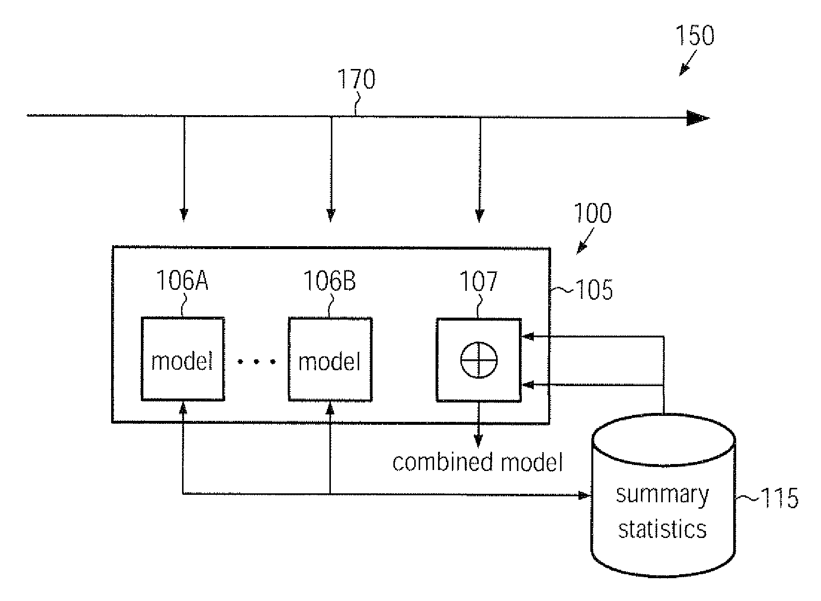
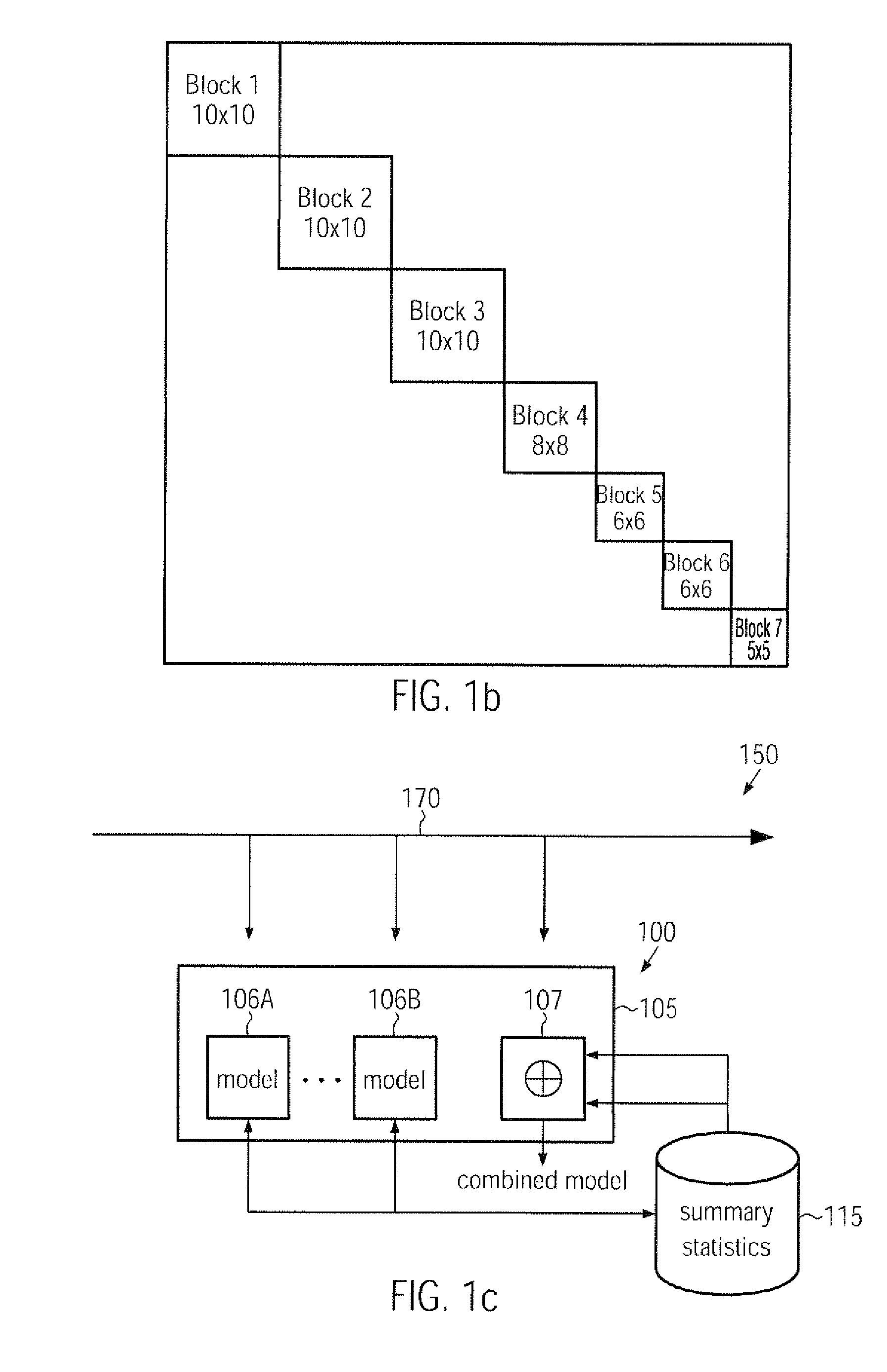
[0016]Generally, the present disclosure relates to methods and systems for fault detection and classification in manufacturing processes for producing semiconductor devices, wherein a significant reduction of PCA models may be accomplished for a given set of parameters to be monitored, thereby enhancing the overall handling of the measurement data substantially without sacrificing the accuracy of the PCA results or even by enhancing the robustness of the corresponding models. To this end, a multi-dimensional parameter set, as may be required for assessing a respective manufacturing environment, may be divided into a plurality of subsets of parameters, which may then be separately modeled, thereby obtaining a low number of summary statistic values. Thereafter, the summary statistic values may be appropriately combined to obtain a combined model for evaluating the initial parameter set as a whole. Since the size of PCA models increases quadratically with the number of parameters, the size of the sum of the individual PCA models is significantly smaller compared to a single PCA model covering the initial entire parameter set.

Problems solved by technology

The latter aspect is especially important since, in modern semiconductor facilities, equipment is required which is extremely cost-intensive and represents the dominant part of the total production costs.
For example, in manufacturing modern integrated circuits, several hundred individual processes may be necessary to complete the integrated circuit, wherein failure in a single process step may result in a loss of the complete integrated circuit.
This problem is even exacerbated in that the size of substrates, on which a plurality of such integrated circuits are processed, steadily increases, so that failure in a single process step may possibly entail the loss of a large number of products.
A corresponding process control, however, is not practical since measuring the effects of certain processes may require relatively long measurement times, frequently ex-situ, or may even necessitate the destruction of the sample.
Moreover, immense effort, in terms of time and equipment, would have to be made on the metrology side to provide the required measurement results.
Furthermore, many of the complex mutual dependencies of the various processes are typically not known, so that a priority determination of respective process specifications may be difficult.
Nevertheless, in total, a large number of dummy substrates or pilot substrates may be necessary to adjust process parameters of respective process tools, wherein tolerable parameter drifts during the process have to be taken into consideration when designing a process sequence, since such parameter drifts may remain undetected over a long time period or may not efficiently be compensated for by SPC techniques.
Even though APC strategies may contribute significantly to yield improvement and / or enhanced device performance and / or a reduction of production costs, nevertheless, a statistical probability exists that even process results obtained by using an APC technique may be outside of predefined value ranges, thereby resulting in yield loss.
In high-volume production lines, even short delays between the occurrence of an out-of-control situation, indicating for instance an equipment failure, and its detection may therefore lead to substantial monetary losses.
As previously explained, several hundred process steps may typically be required for completing sophisticated integrated circuits, wherein each of these steps has to be maintained within specified process margins, wherein, however, the mutual interaction of the highly complex manufacturing processes on the finally obtained electrical performance of the completed device may not be known.
Consequently, even a deviation of the plurality of processes within the specified process windows may result in a significant variation of the finally obtained process result.
Although the respective measurement steps may be restricted to a defined number of samples, the continuously increasing complexity of the overall manufacturing process may require the monitoring of a large number of process parameters, such as layer thicknesses of critical process layers, such as the gate dielectric material and the like, critical dimensions of certain circuit components, such as gate electrodes, doping levels, strain levels, sheet resistivity and the like, wherein many of these process parameters may have to be monitored for a plurality of different device levels, for instance for a plurality of metallization levels and the like.
Consequently, it may be extremely difficult to reliably evaluate the quality of a production process, since taking into consideration only a restricted number of process parameters may result in a less meaningful estimation since the mutual interactions of the various process steps may not be known in advance, while monitoring a high number of process parameters may involve complex data processing algorithms so as to detect relevant parameters and their deviation from target values on the basis of very large data sets.
Although the PCA algorithm provides a powerful tool for detecting faults during the production of semiconductor devices, the number of parameters to be monitored may steadily increase due to the increasing complexity of the overall manufacturing flow, as previously explained.
The increase in model size, however, results in an increase of time and computer memory required to build and update the PCA models.
Consequently, due to the increased number of process steps involved and the increased complexity of the semiconductor equipment, as well as the finally obtained products, an increasing number of parameters has to be monitored, thereby also contributing to an even greater increase of the corresponding PCA models.
Due to the limited resources with respect to storage space and computational power, the creation and updating of PCA models may thus require extremely large resources, thereby rendering the entire PCA strategy for fault detection and classification less attractive.
The KNN model sizes are generally smaller than the respective PCA models but are computationally more demanding and thus require increased computational resources.
Furthermore, the results of KNN fault detection mechanisms are often considerably different compared to the results obtained by PCA, and the interpretation of KNN results is less comprehensive compared to the PCA results.
On the other hand, OMA has the advantage of being computationally efficient and thus inexpensive while, however, the fault detection method may not be as robust compared to PCA mechanisms.
A correlation between at least some of the measured parameters is common in semiconductor manufacturing processes and this is the reason why the OMA method may create many “false alarms.”

Method used


Image

  • Method and system for semiconductor process control and monitoring by using pca models of reduced size
  • Method and system for semiconductor process control and monitoring by using pca models of reduced size
  • Method and system for semiconductor process control and monitoring by using pca models of reduced size

Examples


Embodiment Construction

[0025]Various illustrative embodiments of the invention are described below. In the interest of clarity, not all features of an actual implementation are described in this specification. It will of course be appreciated that in the development of any such actual embodiment, numerous implementation-specific decisions must be made to achieve the developers' specific goals, such as compliance with system-related and business-related constraints, which will vary from one implementation to another. Moreover, it will be appreciated that such a development effort might be complex and time-consuming, but would nevertheless be a routine undertaking for those of ordinary skill in the art having the benefit of this disclosure.

[0026]The present subject matter will now be described with reference to the attached figures. Various structures, systems and devices are schematically depicted in the drawings for purposes of explanation only and so as to not obscure the present disclosure with details ...


PUM


Abstract

By dividing a complex set of parameters of a production process in forming semiconductor devices into individual blocks, respective PCA models may be established for each block and may thereafter be combined by operating on summary statistics of each model block in order to evaluate the complete initial parameter set. Thus, compared to conventional strategies, a significant reduction of the size of the combined PCA model compared to a single PCA model may be obtained, while also achieving an enhanced degree of flexibility in evaluating various subsets of parameters.

Description

BACKGROUND OF THE INVENTION[0001]1. Field of the Invention[0002]The present disclosure generally relates to the field of fabricating semiconductor devices, and, more particularly, to process control and monitoring techniques for manufacturing processes, wherein an improved process control quality is achieved by detecting process failures on the basis of production data.[0003]2. Description of the Related Art[0004]Today's global market forces manufacturers of mass products to offer high quality products at a low price. It is thus important to improve yield and process efficiency to minimize production costs. This holds especially true in the field of semiconductor fabrication, since, here, it is essential to combine cutting-edge technology with mass production techniques. It is, therefore, the goal of semiconductor manufacturers to reduce the consumption of raw materials and consumables while at the same time improve product quality and process tool utilization. The latter aspect is ...

Claims


Application Information

Patent Timeline
IPC IPC(8): G06F19/00G06F17/10G06F17/30G06G7/66
CPCH01L22/20G06K9/6247G06F18/2135
Inventor GOOD, RICHARDKOST, DANIEL
Owner GLOBALFOUNDRIES INC
Learn More