Method and apparatus for removing polymer from a substrate

a technology of polymer and substrate, applied in the field of semiconductor processing systems, can solve the problems of forming defects, becoming a source of particulates, and integrating circuits becoming complex devices

Inactive Publication Date: 2009-11-12
APPLIED MATERIALS INC
View PDF25 Cites 415 Cited by
  • Summary
  • Abstract
  • Description
  • Claims
  • Application Information

AI Technical Summary

Benefits of technology

[0012]In another embodiment, a substrate processing system includes a vacuum transfer chamber having a robot, a etch reactor coupled to the transfer chamber and configured to etch a dielectric material disposed on the substrate, wherein the dielectric material is selected from at least one of silicon oxide and silicon oxycarbide, a polymer removal chamber coupled to the transfer chamber, the robot configured to transfer a substrate between the polymer removal chamber and the etch reactor, the polymer removal chamber having a remote plasma source providing reactive species to an interior of the polymer removal chamber through an outlet port, and a B-field generator disposed in the polymer removal chamber, wherein the B-field generator is configured to provide a B-field at the outlet port that reduces the number of ions touching an edge of a substrate disposed on the substrate support assembly.

Problems solved by technology

Integrated circuits have evolved into complex devices that can include millions of components (e.g., transistors, capacitors and resistors) on a single chip.
As the dimensions of the integrated circuit components are reduced (e.g. to sub-micron dimensions), the importance of reducing presence of contaminant has increased since such contaminant may lead to the formation of defects during the semiconductor fabrication process.
For example, in an etching process, by-products, e.g., polymers that may be generated during the etching process, may become a source of particulate, contaminating integrated circuits and structures formed on the substrate.
Residual polymer present on the substrate bevel may be dislodged and adhered to the front side of the substrate, potentially damaging integrated circuits formed on the front side of the substrate.
In the embodiment wherein residual polymer present on the substrate bevel are dislodged and adhered to a backside of a substrate, non-planarity of the substrate during a lithographic exposure process may result in lithographic depth of focus errors.
Furthermore, residual polymer present on the backside of the substrate may also be dislodged and flaked off during robot transfer process, substrate transport process, subsequent manufacturing processes, and so on, thereby resulting in contamination in transfer chambers, substrate cassettes, process chambers and other processing equipment that may be subsequently utilized in the circuit component manufacturing process.
Contamination of processing equipment results in increased tool down time, thereby adversely increasing the overall manufacturing cost.
However, during the cleaning process, structures formed in the front side of the substrate may also be damaged, resulting in product yield loss and device failure.
However, incomplete removal of the photoresist layer on the front side of the substrate may also contaminant the structures formed on the substrate, resulting in product yield loss and device failure.

Method used


Image

  • Method and apparatus for removing polymer from a substrate
  • Method and apparatus for removing polymer from a substrate
  • Method and apparatus for removing polymer from a substrate

Examples


Embodiment Construction

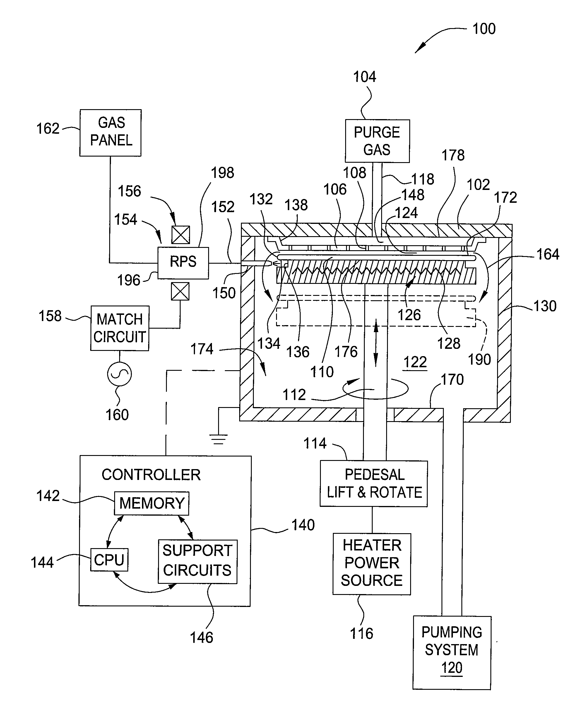
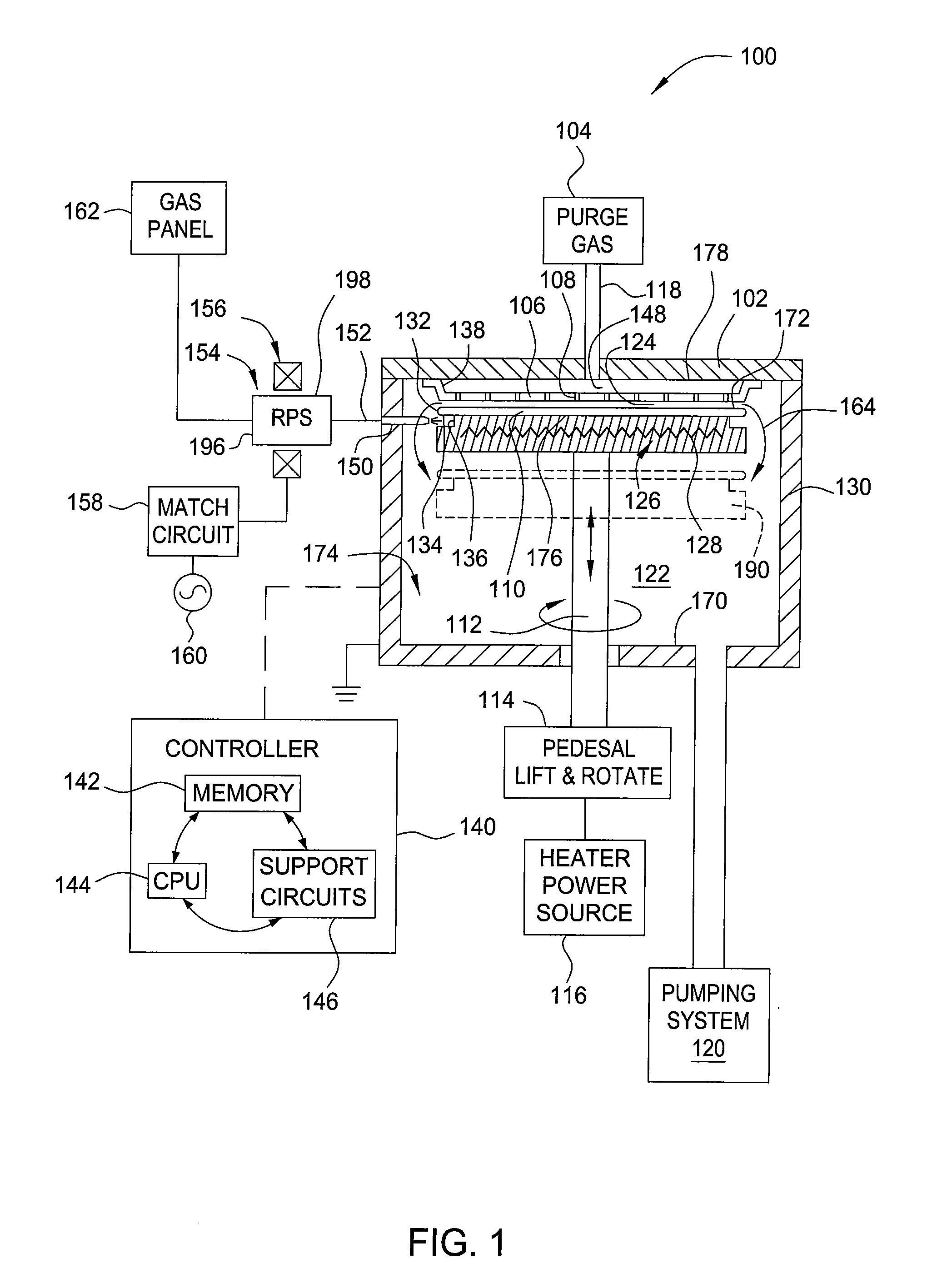
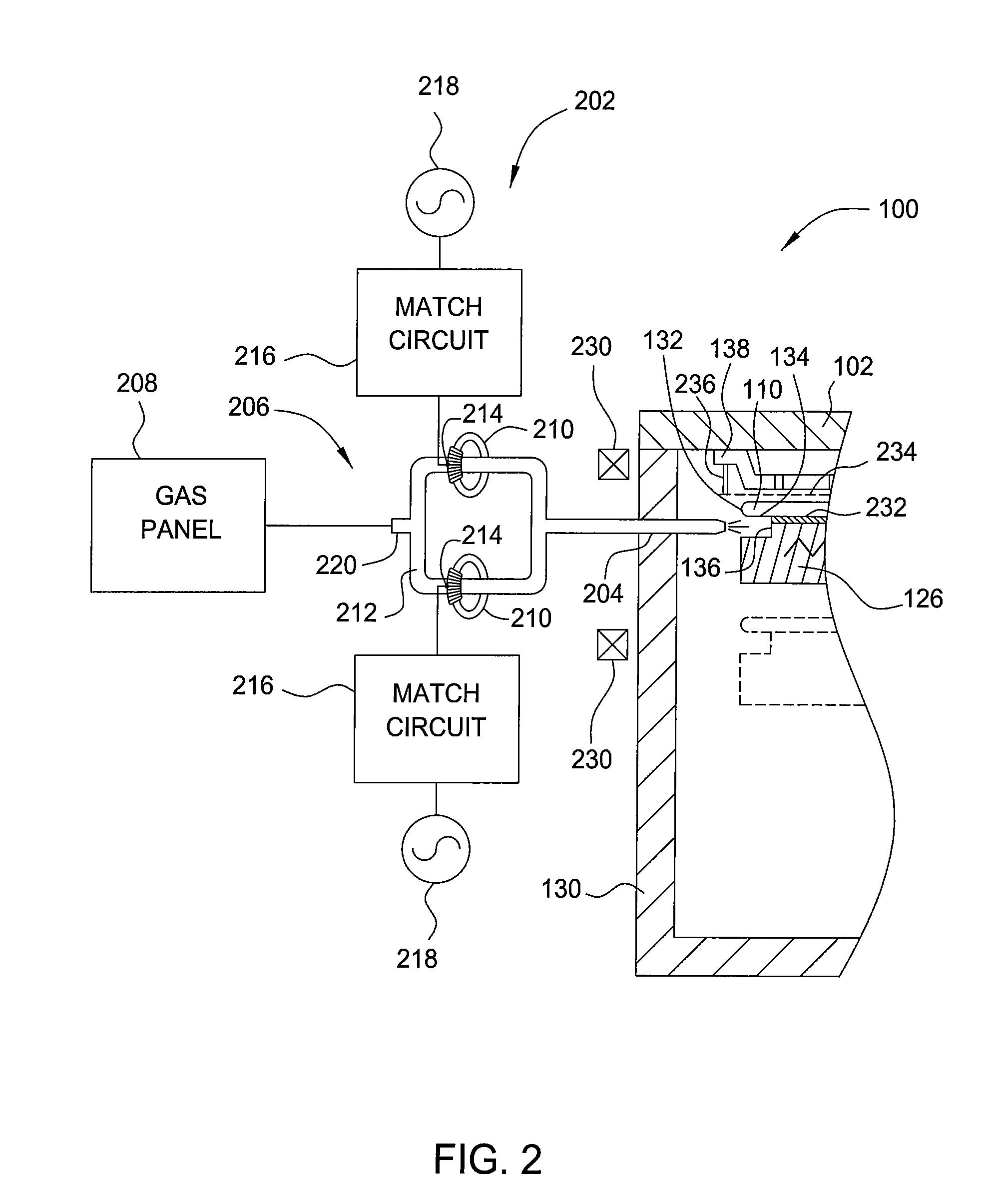
[0022]Embodiments of the present invention include methods and apparatuses that may be utilized to remove polymers from a substrate periphery region, such as an edge or bevel of the substrate. The substrate bevel, backside and substrate periphery region may be efficiently cleaned. In the embodiment wherein a photoresist layer, if any, is present on front side of the substrate, the photoresist layer may be moved as well. In one embodiment, a polymer removal apparatus includes a plasma source fabricated from a hydrogen resistant material. The polymer removal apparatus is generally used to remove polymers from a substrate generated during a semiconductor substrate process, such as an etching or deposition process, among others. One exemplary polymer removal apparatus described herein, with referenced to FIGS. 1-2, is a polymer removal reactor, available from Applied Materials, Inc. of Santa Clara, Calif., and one exemplary substrate processing apparatus described herein, with reference...


PUM

PropertyMeasurementUnit
thickaaaaaaaaaa
frequencyaaaaaaaaaa
frequencyaaaaaaaaaa

Abstract

A method and an apparatus for removing polymer from a substrate are provided. In one embodiment, an apparatus utilized to remove polymer from a substrate includes a processing chamber having a chamber wall and a chamber lid defining a process volume, a substrate support assembly disposed in the processing chamber, a remote plasma source coupled to the processing chamber through an outlet port formed through the processing chamber, the outlet port having an opening pointing toward an periphery region of a substrate disposed on the substrate support assembly, and a substrate supporting surface of the substrate support assembly that substantially electrically floats the substrate disposed thereon relative to the substrate support assembly.

Description

CROSS-REFERENCE TO OTHER APPLICATIONS[0001]This application claims benefit of U.S. Provisional Application Ser. No. 61 / 051,990 filed May 9, 2008 (Attorney Docket No. APPM / 13018L), which is incorporated by reference in its entirety.BACKGROUND[0002]1. Field[0003]Embodiments of the present invention generally relate to a semiconductor processing systems. More specifically, embodiments of the invention relates to a semiconductor processing system utilized to remove polymers from a backside of a substrate in semiconductor fabrication.[0004]2. Description of the Related Art[0005]Integrated circuits have evolved into complex devices that can include millions of components (e.g., transistors, capacitors and resistors) on a single chip. The evolution of chip designs continually requires faster circuitry and greater circuit density. The demands for greater circuit density necessitate a reduction in the dimensions of the integrated circuit components.[0006]As the dimensions of the integrated c...

Claims


Application Information

Patent Timeline
Patent Type & Authority Applications(United States)
IPC IPC(8): B44C1/22C23F1/08
CPCG03F7/427H01J37/32357H01J37/32495H01J37/3266H01L21/67207H01L21/0206H01L21/02087H01L21/0209H01L21/31138H01L21/02057
Inventor RUI, YINGYOUSIF, IMADHOFFMAN, DANIEL
Owner APPLIED MATERIALS INC
Why Eureka
Try Eureka