Semiconductor package enhancing variation of movability at ball terminals

a technology of magnetic and ball terminals, applied in the field of magnetic/solid-state device details, semiconductor devices, electrical devices, etc., can solve the problems of poor product reliability, large impact on the quality of electrical connections, and ball drop or ball crack, so as to improve the quality of the semiconductor package 300, reduce the stress exerted, and increase the thickness of the die-attaching material

Inactive Publication Date: 2009-11-12
POWERTECH TECHNOLOGY
View PDF2 Cites 4 Cited by
  • Summary
  • Abstract
  • Description
  • Claims
  • Application Information

AI Technical Summary

Benefits of technology

[0034]Preferably, as shown in FIG. 7, the chip 330 has a cross-sectional corner 331 in contact with the die-attaching material 320 where the cross-sectional corner 331 is approximately parallel to the second row of ball terminals 350. Furthermore, as shown in FIG. 7 and FIG. 8, the stepwise depression 314 has an edge 314A located outside the die-attaching area 313 adjacent to the cross-sectional corner 331 in parallel to increase the thickness of the die-attaching material 320 measured between the cross-sectional corner 331 and the second row of ball terminals 350 to reduce the stresses exerted by the cross-sectional corner 331 of the chip 230 to the second ball terminals 350.
[0035]Moreover, the stepwise depression 314 can limit and control the flowing of the die-attaching material 320 without bleeding. As shown in FIG. 7, the die-attaching material 320 will not bleed to the sidewalls of the substrate 310 to ensure that the die-attaching material 320 is completely encapsulated by the encapsulant 370. The quality of the semiconductor package 300 is improved.

Problems solved by technology

Furthermore, when a semiconductor package is under operations or under thermal cycle test, TCT, thermal stresses will generate between the semiconductor package and the external printed circuit board due to mismatch of the coefficients of thermal expansion, CTE, where the thermal stresses will exert on the ball terminals, especially on those located at the peripheries or corners of the substrate and close to the edges of IC chips causing substrate warpage and / or solder ball cracks leading to poor product reliability.
Moreover, the impact forces during drop tests will also exert on the second row of ball terminals 150 leading to ball drop or ball crack.
The quality of electrical connections will be greatly affected by the solder ball cracks or dropped balls.
Furthermore, some of the ball terminals 150 located adjacent to the corners of the chip 130 will also have solder ball cracks and ball drop issues due to substrate warpage.

Method used


Image

  • Semiconductor package enhancing variation of movability at ball terminals
  • Semiconductor package enhancing variation of movability at ball terminals
  • Semiconductor package enhancing variation of movability at ball terminals

Examples


first embodiment

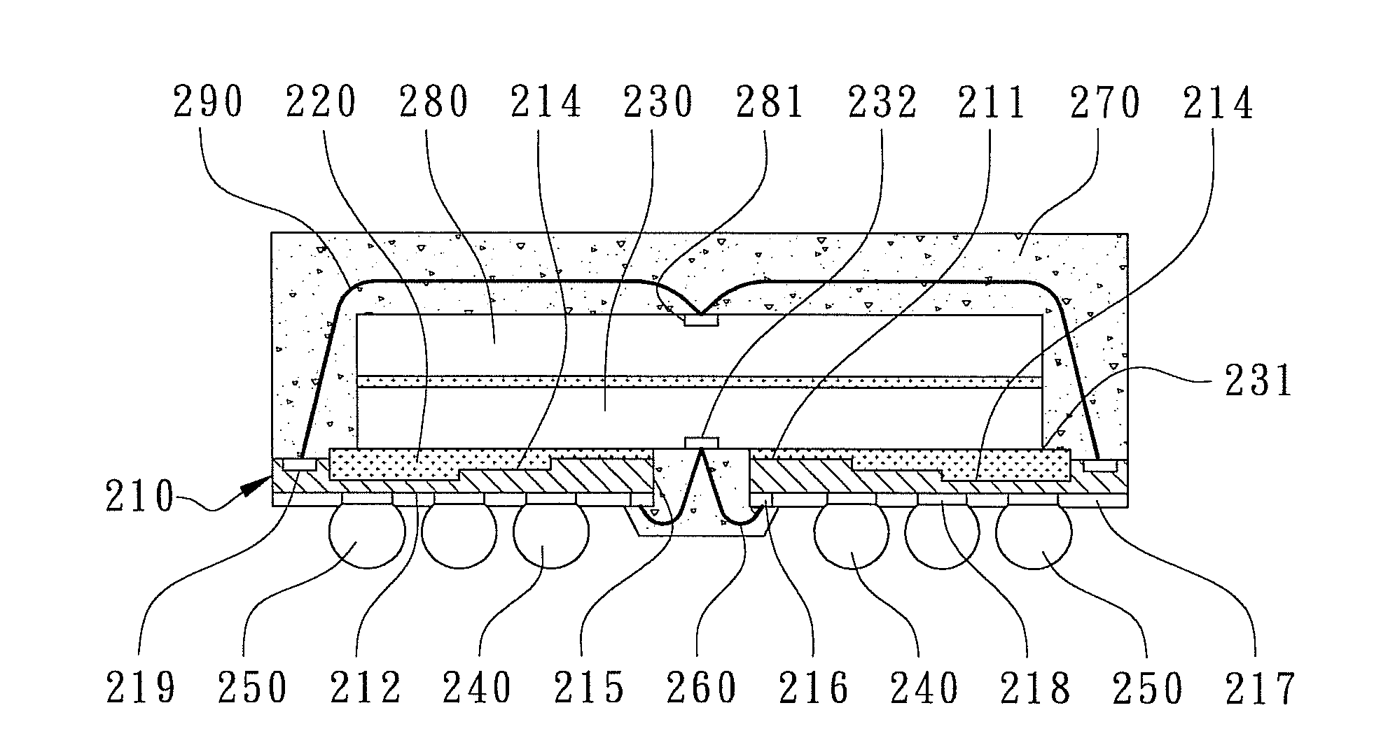
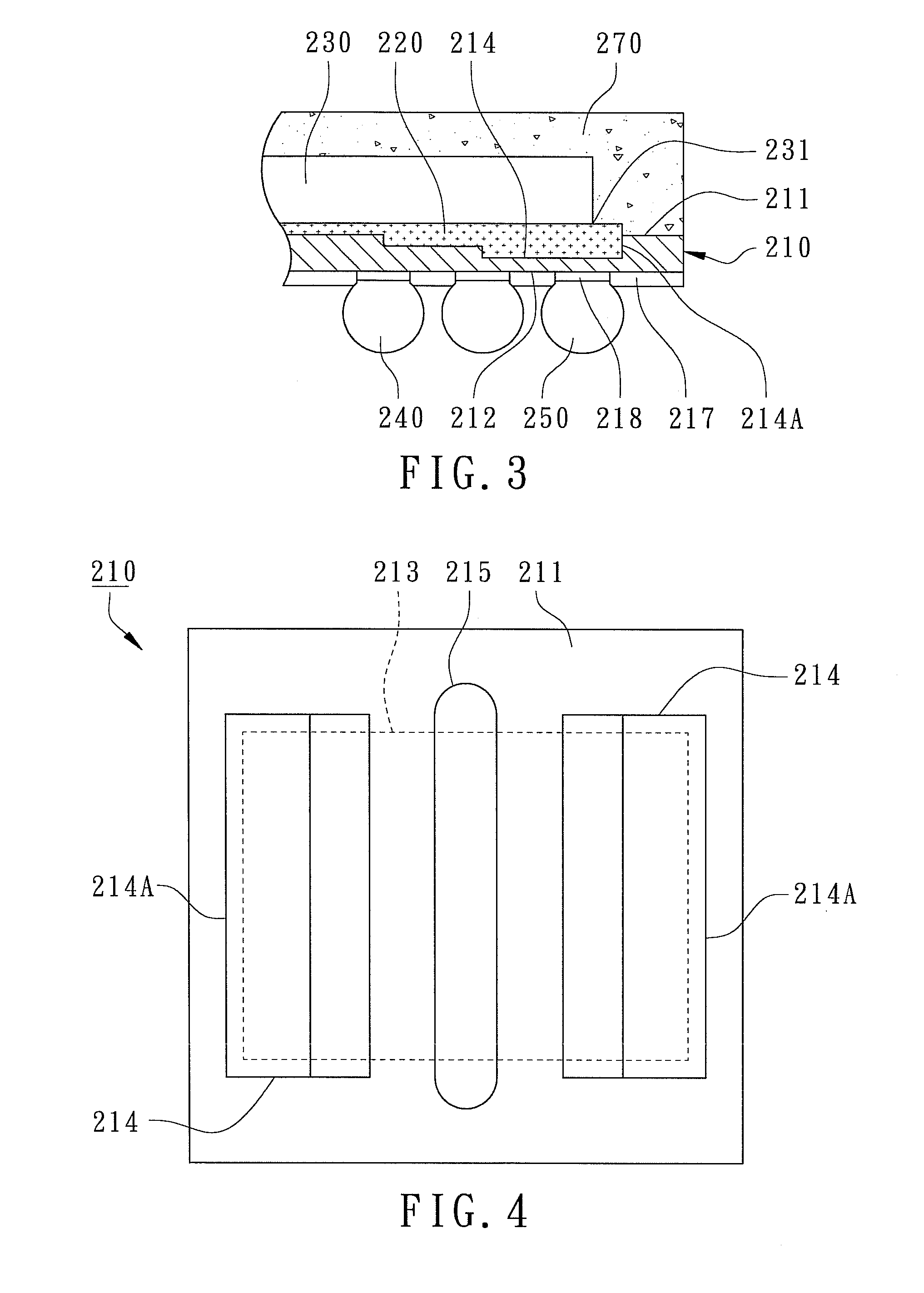
[0018]According to the present invention, a semiconductor package with enhanced mobility of ball terminals is illustrated in the cross-sectional view of FIG. 2 and the partially enlarged cross-sectional view of FIG. 3. The semiconductor package 200 primarily comprises a substrate 210, a die-attaching material 220, a chip 230, a first row of ball terminals 240, and a second row of ball terminals 250. Therein, the substrate 210 is illustrated in the top view of FIG. 4 and the three-dimensional cross-sectional view of FIG. 5.

[0019]The substrate 210 has a covered surface 211, an exposed surface 212, and a slot 215 where the covered surface 211 includes a die-attaching area 213 (as shown in FIG. 4), and the dimension of the die-attaching area 213 is approximately equal to the one of the chip 230. The second ball terminals 250 are linearly disposed in parallel to a central line of the die-attaching area 213 and are relatively further away from the central line of the die-attaching area 21...

third embodiment

[0030]According to the present invention, another semiconductor package with enhanced mobility of ball terminals is revealed as shown in FIG. 7. The semiconductor package 300 primarily comprises a substrate 310, a die-attaching material 320, a chip 330, a first row of ball terminals 340, and a second row of ball terminals 350. The substrate 310 is illustrated in the three-dimensional view of FIG. 8. The substrate 310 has a covered surface 311 and an exposed surface 312 where the covered surface 311 includes a die-attaching area 313, and the dimension of the die-attaching area 313 is approximately equal to the one of the chip 330. A solder mask 317 is formed on the exposed surface 312 of the substrate 310 where the solder mask 317 is an electrically isolated material to protect the traces with the external ball pads 318 exposed for bonding the first row of ball terminals 340 and the second row of ball terminals 350. Furthermore, as shown in FIG. 7 and FIG. 8 again, the substrate 310 ...


PUM


Abstract

A semiconductor package with enhanced mobility of ball terminals is revealed. A chip is attached to the substrate by a die-attaching material where the substrate has at least a stepwise depression on the covered surface to make the substrate thickness be stepwise decreased from a central line of the die-attaching area toward two opposing sides of the substrate. The die-attaching material is filled in the stepwise depression. Therefore, the thickness of the die-attaching material under cross-sectional corner(s) of the chip becomes thicker so that a row of the ball terminals away from the central line of the die-attaching area can have greater mobility without changing the appearance, dimensions, thicknesses of the semiconductor package, nor the placing plane of the ball terminals. Accordingly, the row of ball terminals located adjacent the edges or corners of the semiconductor package can withstand larger stresses without ball cracks nor ball drop. The stepwise depression can accommodate the die-attaching material to control bleeding contaminations.

Description

FIELD OF THE INVENTION[0001]The present invention relates to a semiconductor device with semiconductor packaging technologies, especially to a semiconductor package with enhanced mobility of ball terminals.BACKGROUND OF THE INVENTION[0002]There are different types of semiconductor packages for different electronic products such as Ball Grid Array, BGA, having a plurality of ball terminals such as solder balls disposed at the bottoms of the semiconductor packages. Normally, the ball terminals should be formed on an exposed surface of a substrate by reflowing with sufficient numbers to be I / O connecting terminals for the semiconductor packages to electrically connect to an external printed circuit board for operations and to meet the high-density SMT requirements. During semiconductor packaging processes, substrates experience different heat treatments such as curing of die-attaching materials and encapsulant and reflowing of ball terminals. Furthermore, when a semiconductor package i...

Claims


Application Information

Patent Timeline
Patent Type & Authority Applications(United States)
IPC IPC(8): H01L23/498
CPCH01L23/13H01L2224/06136H01L2224/32145H01L2224/32225H01L2224/48091H01L2224/4824H01L2224/73215H01L2224/73265H01L2224/83385H01L2924/01005H01L2924/01082H01L2924/14H01L2924/15311H01L25/0657H01L2224/06135H01L2225/06565H01L2225/06558H01L2225/0651H01L2924/01033H01L24/48H01L24/32H01L2924/00014H01L2924/00H01L2924/3512H01L2924/351H01L2924/181H01L2224/26175H01L2924/00012H01L2224/45099H01L2224/45015H01L2924/207
Inventor FAN, WEN-JENG
Owner POWERTECH TECHNOLOGY
Why Eureka
Try Eureka