Electronic component and resin packaging method for electronic component

a technology of electronic components and resins, applied in the direction of resistive material coating, liquid/solution decomposition chemical coating, superimposed coating process, etc., can solve the problems of inability to reduce malfunction of the electronic component, etc., to reduce the mounding of the resin, and the overall height of the electronic component can be restricted

Active Publication Date: 2009-11-12
PANASONIC CORP
View PDF17 Cites 8 Cited by
  • Summary
  • Abstract
  • Description
  • Claims
  • Application Information

AI Technical Summary

Benefits of technology

[0021]In the present invention, since the second sealing resin which is softer than the first sealing resin is positioned to the inner side of the first sealing resin which surrounds the outer perimeter section of the component, then it is possible to reduce mounding of the resin corresponding to the outer perimeter edge portion of the component. Moreover, by chamfering a portion or all of an edge, in the vicinity where the wire passes, of edge portions of the outer perimeter of the component and by providing the wire so as to extend to the board along the chamfered oblique surface, it is possible further to reduce mounding of the resin and therefore the overall height of the electronic component can be restricted.
[0022]Furthermore, when sealing the component installed on the board by means of resin, since a first sealing resin is supplied and cured so as to surround the outer perimeter portion of the component whereupon a second sealing resin having a lower viscosity than the first viscosity is filled and cured within the periphery of the first sealing resin, it is possible to reduce mounding corresponding to

Problems solved by technology

In view of these circumstances, if wires make contact with the edge portions of the component, there are problems in that shorting between mutually adjacent wires occurs via the conductive film on the component, and malfunction of the electronic

Method used


Image

  • Electronic component and resin packaging method for electronic component
  • Electronic component and resin packaging method for electronic component
  • Electronic component and resin packaging method for electronic component

Examples


first embodiment

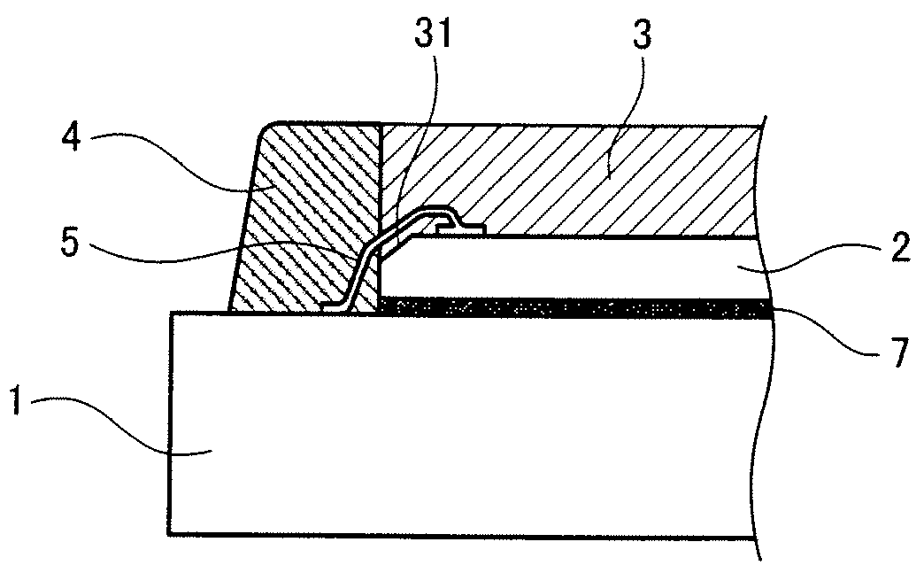
[0047]FIGS. 1A and 1B to FIG. 4 show a first embodiment of the present invention.

[0048]FIG. 1A shows an electronic component according to the present invention.

[0049]In this electronic component, a semiconductor chip 2, which is a component, is die bonded by a die attach film 7 to the upper surface of a circuit board 1, and an electrode of the semiconductor chip 2 and an electrode of the board 1 are bonded by a wire 5.

[0050]A resin package is formed by supplying and curing a first sealing resin 4 so as to surround the outer perimeter portion of the semiconductor chip 2 on the upper surface of the board 1, and then filling and curing a second sealing resin 3 inside the first sealing resin 4 so as to cover the semiconductor chip 2.

[0051]The viscosity of the second sealing resin 3 during filling is lower than the viscosity of the first sealing resin 4 during filling, while the coefficient of elasticity of the second sealing resin 3 after curing is lower than the coefficient of elastici...

second embodiment

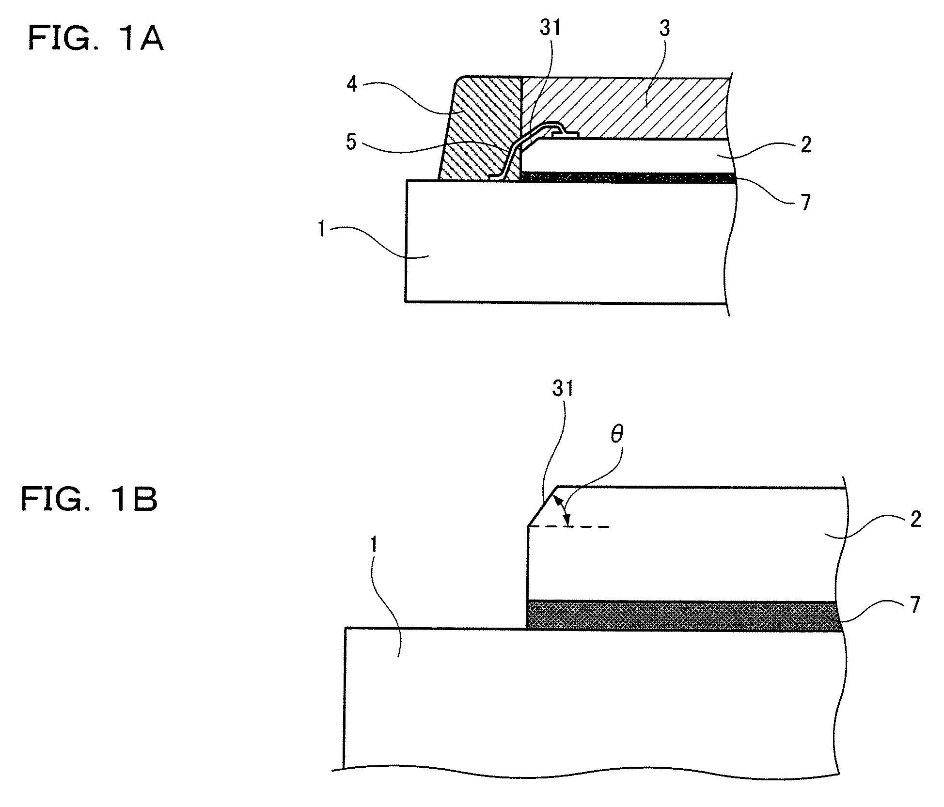
[0074]FIG. 5A, FIG. 5B and FIG. 5C show a second embodiment of the present invention.

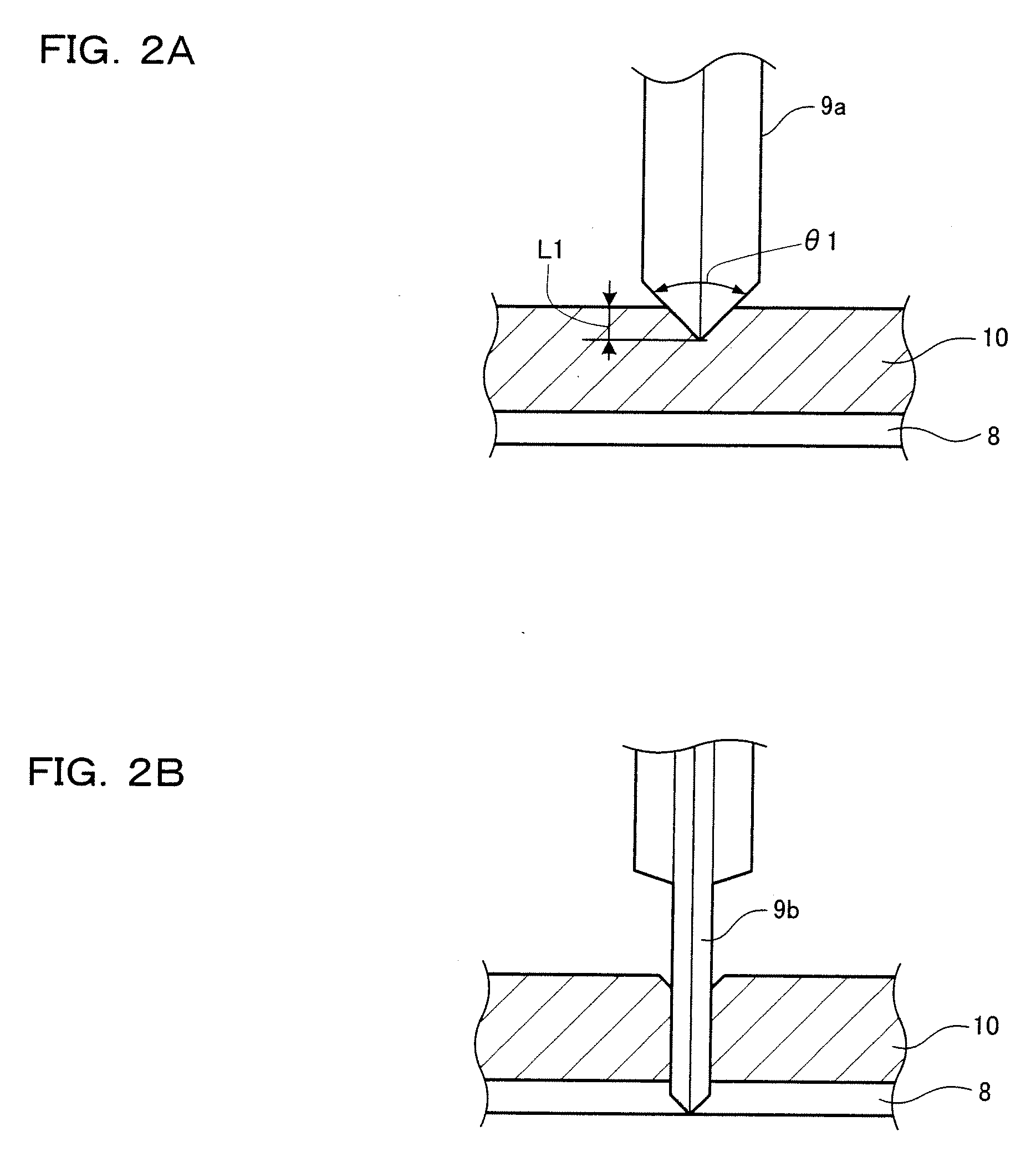
[0075]The point of difference with respect to the first embodiment is that when dicing a semiconductor chip 2 from a wafer, two cutter blades 9c and 9f having different blade tip angles are used, and a two-stage processed shape is formed by firstly carrying out first stage processing using the cutter blade 9c having a larger blade tip angle (FIG. 5A) and then carrying out second stage processing using the cutter blade 9f having a smaller blade tip angle (FIG. 5B).

[0076]More specifically, the blade tip angle of the cutter blade 9c is 135° and the blade tip angle of the cutter blade 9f is 90°.

[0077]As shown in FIG. 1, when the electrode on the board 1 side is close to the outer perimeter of the semiconductor chip 2, then the wire 5 may have a double bend shape and in cases such as this, the height of the wire 5 can be lowered further by processing the oblique surface 31 in two stages so as to have a g...

third embodiment

[0080]FIGS. 6A to 6E show a third embodiment of the present invention.

[0081]In the first embodiment and the second embodiment, a cutter blade was used when fabricating a semiconductor chip 2 from a wafer, but the present embodiment differs from this in that etching is used.

[0082]As shown in FIG. 6A, a semiconductor chip 10 in the form of a wafer is attached to a sheet 8, and in this state a first resist 20 is formed on the surface of the semiconductor chip 10. An opening section 22 is etched using an etching solution. Holes with good S / N, in other words, large depth compared to the hole diameter, are formed using a solution having a high etching rate (FIG. 6B).

[0083]Thereupon, as shown in FIG. 6C, the first resist 20 is removed and a second resist 21 is formed. An opening section 23 which is larger than the opening section 22 is formed. Etching is then performed using an etching solution (FIG. 6D). The etching solution used has a low etching rate and performs shallow etching.

[0084]C...


PUM

PropertyMeasurementUnit
Temperatureaaaaaaaaaa
Viscosityaaaaaaaaaa
Heightaaaaaaaaaa

Abstract

An electronic component, in which the outer perimeter portion of a component (2) is surrounded with a first sealing resin (4), a second sealing resin (3) is filled within the periphery of the first sealing resin (4), the component (2) and a board (1) are electrically connected by a wire (5), the edge, in the vicinity of which the wire (5) passes, of the outer perimeter edge portions of the component (2) is formed to be a chamfered oblique surface (31), and the wire (5) is provided to extend to the board (1) along the oblique surface (31). By this means, the overall height of the electronic component can be kept low.

Description

BACKGROUND OF THE INVENTION[0001]1. Field of the Invention[0002]The present invention relates to an electronic component packaged with resin.[0003]2. Description of the Related Art[0004]In recent years, progress has been made in reducing the thickness of electronic component packages. For example, in the case of circuit boards which are used in memory cards, it is essential to reduce thickness due to the restriction on the thickness dimensions of the product. Therefore, it has been necessary to reduce the respective thicknesses of the circuit board, electronic components, wires, resin, cover and the like, which are the constituent components of the product.[0005]In view of these circumstances, if wires make contact with the edge portions of the component, there are problems in that shorting between mutually adjacent wires occurs via the conductive film on the component, and malfunction of the electronic component occurs due to leaking into the component of the signals flowing in the...

Claims


Application Information

Patent Timeline
IPC IPC(8): H01L23/28B32B3/02H05K3/00
CPCH01L21/56H01L2924/01006H01L23/3135H01L24/48H01L2224/45015H01L2224/4809H01L2224/48095H01L2224/48227H01L2224/48465H01L2224/73265H01L2224/85148H01L2924/01004H01L2924/01005H01L2924/01027H01L2924/01033H01L2924/0105H01L2924/01078H01L2924/01079H01L2924/01082H01L2924/10157H01L2924/1815H01L2924/20752H01L23/3121H01L24/45H01L2224/45144H01L2224/32225H01L2924/00014H01L2924/00012H01L2924/00H01L24/73H01L2224/8592H01L2924/10156H01L2924/181H01L2224/85399H01L2224/05599
Inventor IMANISHI, MAKOTOTOMURA, YOSHIHIROKUMAZAWA, KENTARO
Owner PANASONIC CORP
Why Eureka
Try Eureka