Cmp pad thickness and profile monitoring system

a technology of profile monitoring and cmp pad, which is applied in the direction of abrasive surface conditioning devices, lapping machines, instruments, etc., can solve the problems of general decrease of the polishing potential of the processing pad, scratches in the substrate surface, and abraded portions of the pad, so as to restore the effect of restoring the polishing performance of the semiconductor substrate processing surfa

Active Publication Date: 2009-11-12
APPLIED MATERIALS INC
View PDF12 Cites 17 Cited by
  • Summary
  • Abstract
  • Description
  • Claims
  • Application Information

AI Technical Summary

Benefits of technology

[0009]In one embodiment a method is provided for maintaining a semiconductor substrate processing surface. The method generally includes performing a first set of measurements on the semiconductor substrate processing surface, wherein the set of measurements are taken using a displacement sensor coupled to a processing surface conditioning arm, determining a processing surface profile based on the set of measurements, comparing the processing surface profile to a “minimum profile threshold” or “reference profile”, and communicating a result of the profile comparison.
[0010]In one embodiment an apparatus is provided for maintaining a semiconductor substrate processing surface. The apparatus generally includes a semiconductor substrate processing surface for removing material from the semiconductor substrate, a conditioning head for restoring polishing performance of the semiconductor substrate processing surface, a conditioning arm for positioning the conditioning head in contact with the semiconductor substrate processing surface, and a displacement sensor coupled to the conditioning arm. The displacement sensor may be configured to perform a set of measurements on the semiconductor substrate processing surface, determine a processing surface profile based on the set of measurements, compare the processing surface profile to a minimum profile threshold and communicate a result of the profile comparison.
[0011]In one embodiment a system is provided for maintaining a semiconductor substrate processing surface. The system generally includes a semiconductor substrate processing surface for removing material from the semiconductor substrate, a conductive platen for rotating the semiconductor substrate processing surface, a conditioning head for restoring polishing performance of the semiconductor substrate processing surface, a conditioning arm for positioning the conditioning head in contact with the semiconductor substrate processing surface, and a displacement sensor coupled to the conditioning arm.

Problems solved by technology

Such defects may be scratches in the substrate surface caused by raised areas of the pad or by polishing by-products disposed on the surface of the pad, such as accumulation of conductive material removed from the substrate precipitating out of the electrolyte solution, abraded portions of the pad, agglomerations of abrasive particles from a polishing slurry, and the like.
The polishing potential of the processing pad generally decreases during polishing due to wear and / or accumulation of polishing by-products on the pad surface, resulting in sub-optimum polishing qualities.

Method used


Image

  • Cmp pad thickness and profile monitoring system
  • Cmp pad thickness and profile monitoring system
  • Cmp pad thickness and profile monitoring system

Examples


Embodiment Construction

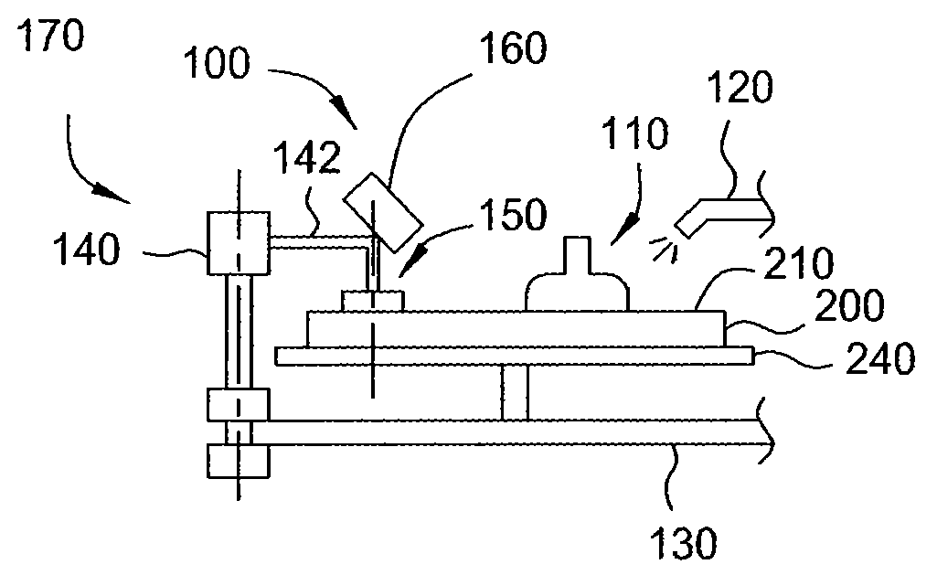
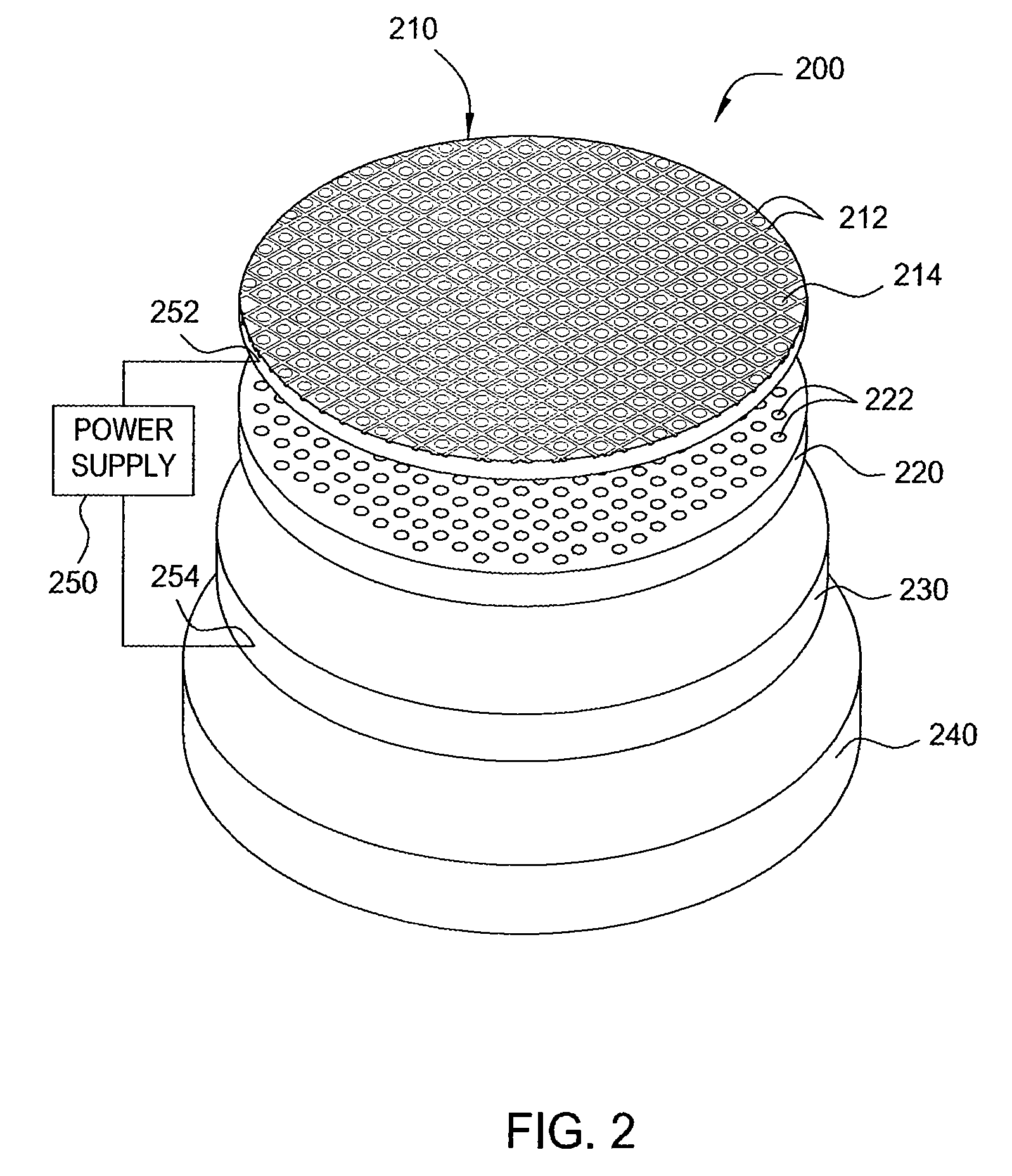
[0019]Embodiments of the invention generally relate to polishing or planarizing processes performed in the production of semiconductor substrates. Electrochemical Mechanical Planarization (ECMP) is one of the polishing processes described and broadly includes removal of previously deposited material from the semiconductor surface by a combination of mechanical, chemical and / or electrochemical forces. The mechanical force may include, but is not limited to, physical contact or rubbing action, and the chemical and / or electrical forces may include, but are not limited to, removal of material by anodic dissolution.

[0020]The substrate typically begins the planarization process having bulk conductive material deposited thereon in a non-planar orientation, portions of which may be removed by one or more ECMP processes in an effort to achieve a planar orientation. The processing pad performing this bulk removal must have the appropriate mechanical properties (e.g., magnitude and structure o...


PUM


Abstract

In one embodiment a method is provided for maintaining a substrate processing surface. The method generally includes performing a set of measurements on the substrate processing surface, wherein the set of measurements are taken using a displacement sensor coupled to a processing surface conditioning arm, determining a processing surface profile based on the set of measurements, comparing the processing surface profile to a minimum profile threshold, and communicating a result of the profile comparison.

Description

CROSS-REFERENCE TO RELATED APPLICATIONS[0001]This application claims benefit of U.S. provisional patent application Ser. No. 61 / 051,634, filed May 8, 2008, which is herein incorporated by reference in its entirety.BACKGROUND OF THE INVENTION[0002]1. Field of the Invention[0003]Embodiments of the invention generally relate to removing material from a substrate. More particularly, embodiments of the invention relate to polishing or planarizing a substrate by electrochemical mechanical polishing.[0004]2. Description of the Related Art[0005]In the manufacture of integrated circuits, layers of conductive material are sequentially deposited on a semiconductor wafer and removed to produce a desired circuit on the wafer.[0006]Chemical Mechanical Processing (CMP) is a technique used to remove conductive materials from a semiconductor wafer or substrate surface by chemical dissolution while concurrently polishing the substrate with downforce and mechanical abrasion. Electrochemical Mechanical...

Claims


Application Information

Patent Timeline
Patent Type & Authority Applications(United States)
IPC IPC(8): H01L21/66B24B49/02B24B49/10B24B37/04
CPCB24B37/042B24B53/12B24B53/017
Inventor MANENS, ANTOINE P.HSU, WEI-YUNGM'SAAD, HICHEM
Owner APPLIED MATERIALS INC
Why Eureka
Try Eureka