Design method of semiconductor package substrate

a technology of semiconductor packaging and substrate, applied in the direction of cad circuit design, program control, instruments, etc., can solve the problems of adverse effect, limited amount of elements which can be added to the printed circuit board, performance degradation, etc., and achieve excellent signal performance and deteriorated signal transmission properties.

Inactive Publication Date: 2009-11-19
RENESAS ELECTRONICS CORP
View PDF11 Cites 3 Cited by
  • Summary
  • Abstract
  • Description
  • Claims
  • Application Information

AI Technical Summary

Benefits of technology

[0017]The second problem lies in an adverse effect that is brought about because the unnecessary element structure exists in transmission lines. The capacitor elements in the above-mentioned technique are generated by adding branches such as openings or short-circuits in middle positions of the original necessary transmission lines. However, it is known that those branches operate as stubs so that the signal transmission property is deteriorated.
[0018]In a reference technique of the present invention, each of individual structural parts in a signal transmission line is adjusted to the standard impedance of 50Ω. By such a design, the entire impedance of the signal transmission line is adjusted to become close to 50Ω in the reference technique. In an aspect of the present invention, the standard impedance of 50Ω is not significant. This is because the signal transmission line in the present invention is designed such that, even if the impedance is deviated from the standard value, the reflected signal wave caused by the deviation is cancelled by another reflected signal wave. In order to achieve such a design, in an aspect of the present invention, individual structural parts in a signal transmission line are intentionally designed to be deviated from a standard impedance reversely as necessary, under a careful control. With such design, the impedance of the signal transmission line is matched with the input / output impedance of the connected semiconductor element. As a result, as the component composed of the semiconductor element and the semiconductor package substrate on which the semiconductor is primarily mounted, a terminal impedance is adjusted to 50Ω. Thus, an excellent signal performance is obtained.

Problems solved by technology

However, when this technique is applied to high speed signal devices exemplified by the SerDes (SERializer / DESerializer, serial / parallel mutual conversion circuit), there are essentially two problems.
The first problem lies in the fact that the element which can be added onto a printed circuit board is limited to capacitor elements.
As a result, contrary to an intension of the technique, the performance is deteriorated.
The second problem lies in an adverse effect that is brought about because the unnecessary element structure exists in transmission lines.
However, it is known that those branches operate as stubs so that the signal transmission property is deteriorated.

Method used


Image

  • Design method of semiconductor package substrate
  • Design method of semiconductor package substrate
  • Design method of semiconductor package substrate

Examples


Embodiment Construction

[0054]The invention will be now described herein with reference to illustrative embodiments. Those skilled in the art will recognize that many alternative embodiments can be accomplished using the teachings of the present invention and that the invention is not limited to the embodiments illustrated for explanatory purposes.

[0055]A design method of a semiconductor package substrate, a semiconductor package substrate design support apparatus and a semiconductor package substrate according to embodiments of the present invention will be described below with reference to the attached drawings.

[0056]The semiconductor package substrate according to embodiments of a present invention can be designed by a semiconductor package substrate design support apparatus according to embodiments of the present invention, by using the semiconductor package substrate design method according to embodiments of the present invention.

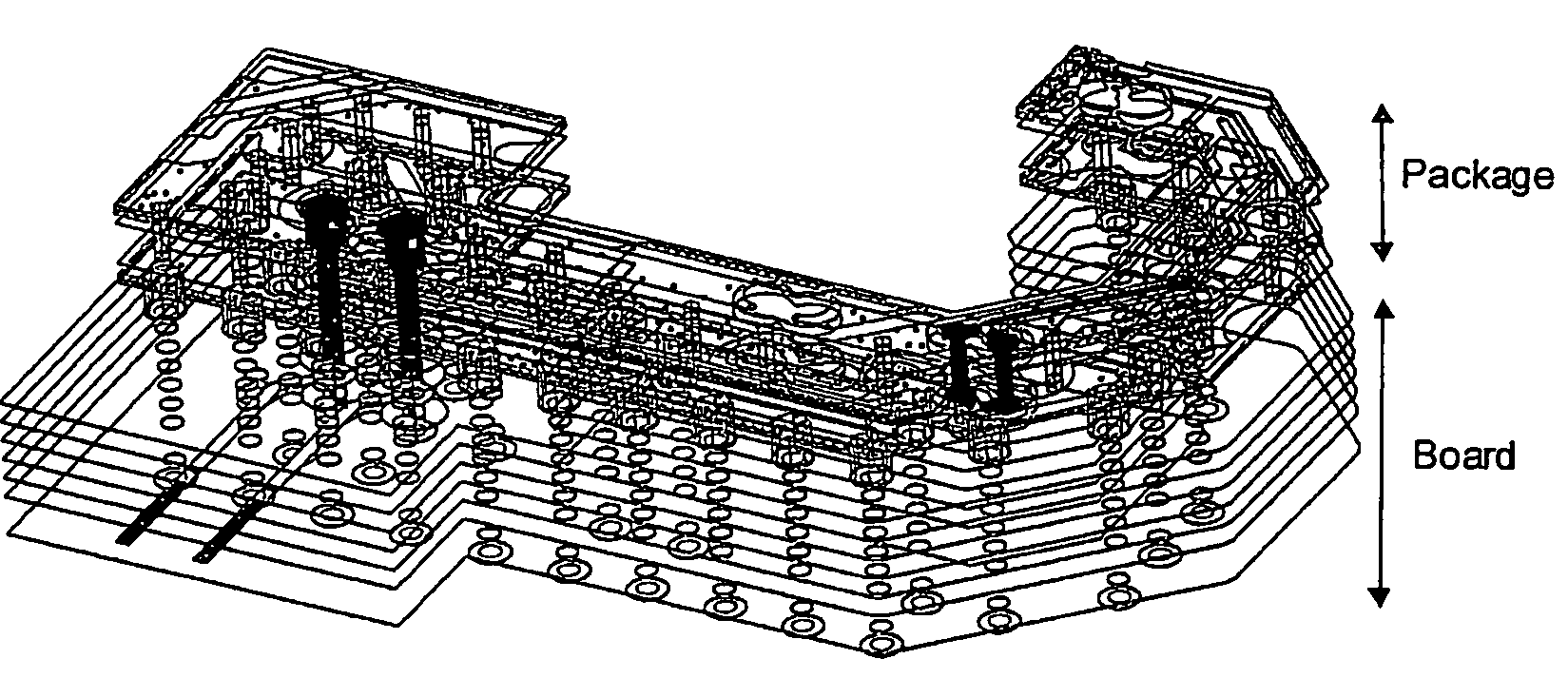
[0057]FIG. 1 is a conceptual view of a semiconductor package substrate d...


PUM


Abstract

When the impedance of a first circuit is deviated from a standard value, a second circuit is designed for generating a second reflected wave to cancel a first reflected wave generated by the first circuit. Individual structural parts in a transmission line are intentionally designed to be deviated from a standard impedance reversely under a fine control. By this method, the impedance matching between the input and output impedance of the semiconductor element and the transmission line is achieved. As a result, the terminal impedance of the component of the semiconductor circuit and the semiconductor package substrate is adjusted to 50 Ohm, so that a good signal property can be obtained.

Description

INCORPORATION BY REFERENCE[0001]This patent application is based on Japanese Patent Application No. 2008-125517. The disclosure of the Japanese Patent Application is incorporated herein by reference.BACKGROUND OF THE INVENTION[0002]1. Field of the Invention[0003]The present invention relates to a semiconductor package substrate, a design method thereof, a manufacturing method thereof and design support apparatus thereof. More particularly, the present invention relates to a semiconductor package substrate on which a semiconductor chip is primarily mounted and which is secondly mounted on a secondary mounting substrate, and a designing method thereof, a manufacturing method thereof, and a design support apparatus for supporting the design thereof.[0004]2. Description of Related Art[0005]In a connection portion of a semiconductor chip and a semiconductor package substrate primarily mounting the semiconductor chip, the impedance matching between the input and output of both units is im...

Claims


Application Information

Patent Timeline
Patent Type & Authority Applications(United States)
IPC IPC(8): H01L23/52G06F17/50H01L21/02
CPCG06F17/5068G06F2217/40H01L23/66H01L27/0207H01L28/40H01L2223/6627H01L2223/6655H01L2924/0002H01L2924/1903H01L2924/19051H01L2924/3011H01L2924/00G06F30/39G06F2113/18
Inventor OIKAWA, RYUICHI
Owner RENESAS ELECTRONICS CORP
Why Eureka
Try Eureka