Semiconductor device and method for manufacturing the same

a semiconductor device and semiconductor technology, applied in the direction of semiconductor devices, semiconductor/solid-state device details, electrical devices, etc., can solve the problems of warpage difficult to provide high-yield, high-reliability, high-density semiconductor devices, etc., to simplify the method of manufacturing the semiconductor device and improve the device characteristics and reliability. , the effect of improving the reliability

Active Publication Date: 2009-11-19
RENESAS ELECTRONICS CORP
View PDF4 Cites 42 Cited by
  • Summary
  • Abstract
  • Description
  • Claims
  • Application Information

AI Technical Summary

Benefits of technology

[0090]According to the present invention, it is possible to provide a high-density, thin semiconductor device superior in device characteristics and reliability, and a simplified method for manufacturing the semiconductor device.

Problems solved by technology

However, the above-described related arts have the below-described problems.
In addition, it is difficult to provide a high-yield, high-reliability, high-density semiconductor device since connecting parts are liable to break down.
In such a structure as described above, if an interconnect structure containing a resin insulating layer is provided on only one side surface for thinning purposes in particular, warpage is liable to occur due to a difference in the contraction percentage of a resin material.
If warpage takes place, defects tend to occur in connecting parts between the semiconductor chip and an interconnect.
In addition, it becomes difficult to mount this semiconductor chip-equipped substrate onto another substrate.
Furthermore, a stress arises in the semiconductor chip, thus possibly causing a degradation in device characteristics.
If the frame material or the substrate having a concave portion is thickened or a reinforcing plate is provided in an attempt to suppress such warpage, it becomes difficult to thin down the semiconductor device.
In addition to such a warpage problem as described above, the structure having the frame material made of resin has the problem of poor heat radiation characteristics since the semiconductor chip, which is a source of heat generation, is surrounded by a resin composing the multilayer interconnect structure and a resin composing the frame material.

Method used


Image

  • Semiconductor device and method for manufacturing the same
  • Semiconductor device and method for manufacturing the same
  • Semiconductor device and method for manufacturing the same

Examples


first exemplary embodiment

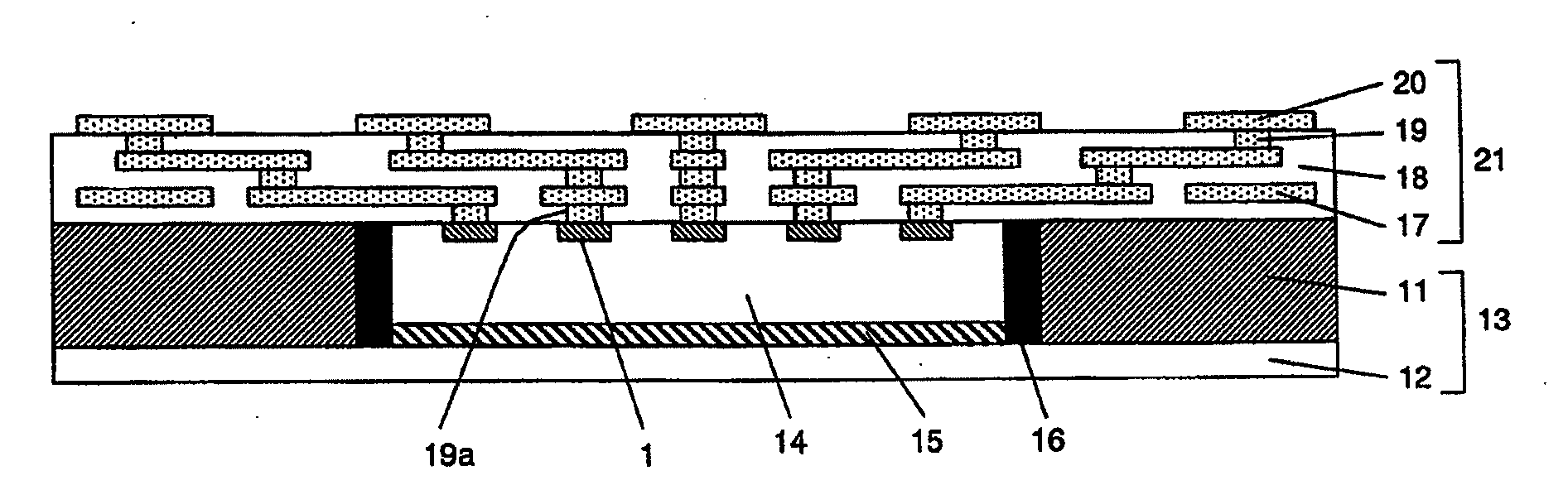
[0114]FIG. 1 is a schematic cross-sectional view illustrating one example of the configuration of a semiconductor device of the present invention. In the configuration shown in FIG. 1, a semiconductor chip 14 is mounted within the concave portion of a base material 13 composed of a metal frame 11 and a resin layer 12 through an adhesion layer 15. An insulating material is filled in a trench between this semiconductor chip 14 and the metal frame 11 and, thus, a filling layer 16 is formed. In addition, an interconnect structure 21 is provided on the base material 13 in which the semiconductor chip 14 is mounted.

[0115]In this interconnect structure 21, an interconnect layer 17 is formed with intervention of an insulating layer 18, and an upper-layer side interconnect and a lower-layer side interconnect are electrically connected to each other through a via. An external terminal 1 of the semiconductor chip is electrically connected to the upper-layer side interconnect layer 17 through a...

second exemplary embodiment

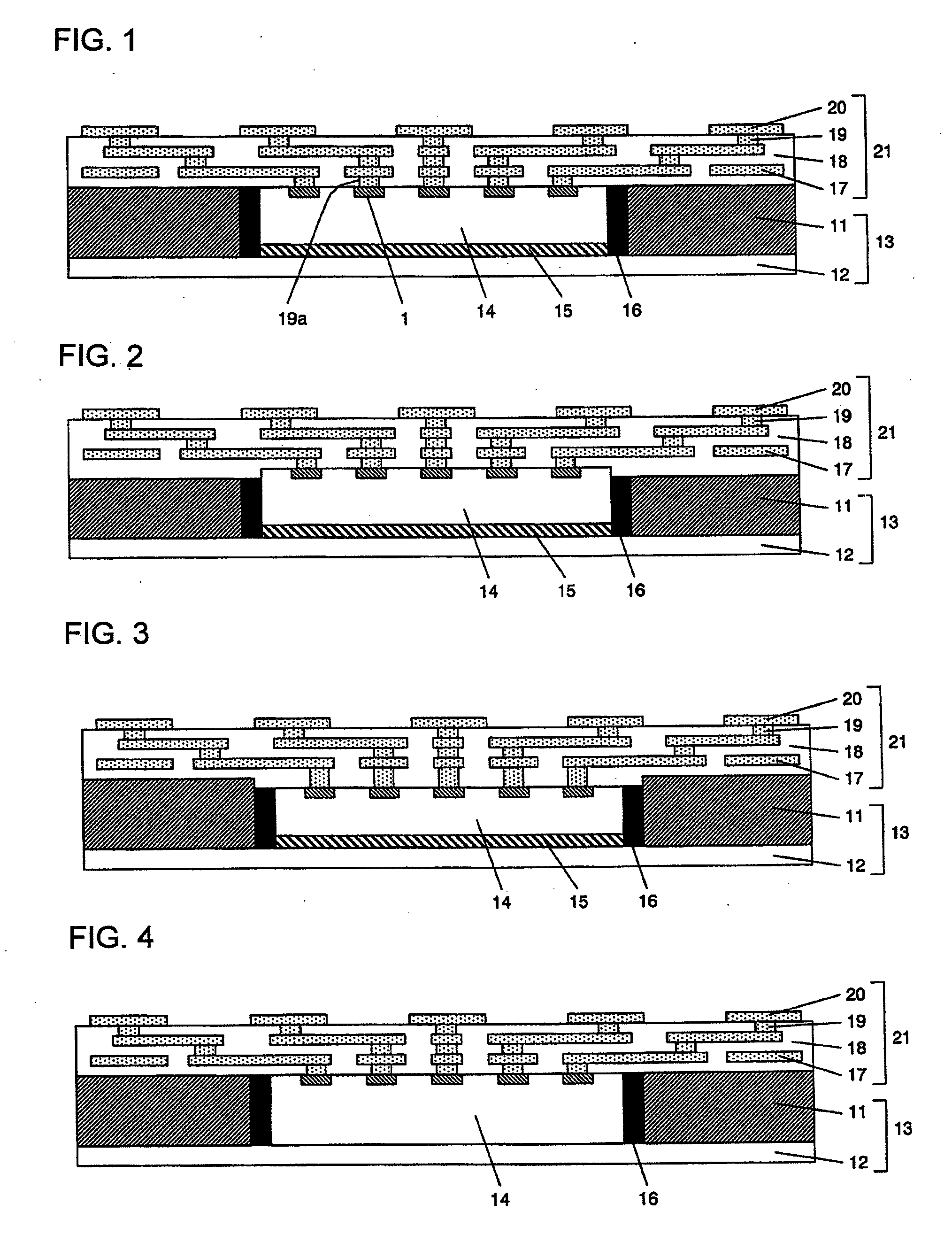
[0140]FIG. 7 is a schematic cross-sectional view illustrating another exemplary embodiment of the configuration of a semiconductor device of the present invention. The present exemplary embodiment differs from the first exemplary embodiment in that the metal frame 11 is electrically connected to an interconnect layer of the interconnect structure 21. The rest of the configuration is the same as that of the first exemplary embodiment. In addition, this configuration may be combined with any of the configurations shown in FIGS. 2 to 6, as described in the first exemplary embodiment.

[0141]In the interconnect structure 21, the metal frame 11, the circuit of the semiconductor chip 14 and the external terminal 20 are electrically connected to one another through the vias 19 and 19b and the interconnect layers provided within the insulating layer 18.

[0142]The via 19b for electrically connecting the metal frame 11 and the interconnect structure 21 can be formed, for example, in the followin...

third exemplary embodiment

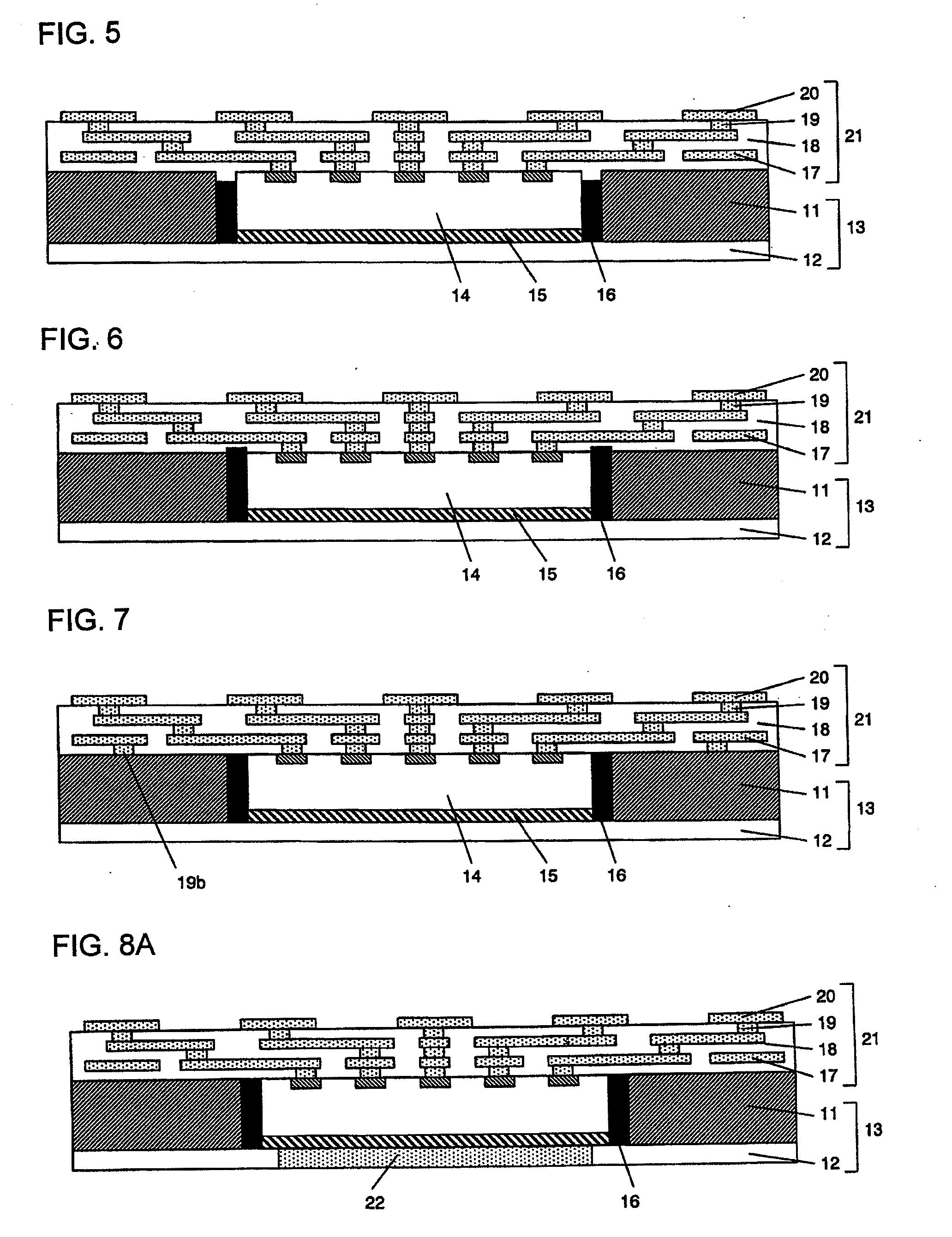
[0144]FIGS. 8A, 8B, 9A, 9B and 9C are schematic explanatory drawings illustrating another exemplary embodiment of a semiconductor device of the present invention. FIGS. 8A and 9A are cross-sectional views, whereas FIGS. 8B, 9B and 9C are perspective views taken from the lower-surface side of the semiconductor device. The present exemplary embodiment differs from the first exemplary embodiment in that a penetrating metal pattern 22 is provided in an organic resin layer 12. For the rest of the present exemplary embodiment, it is possible to apply the same configuration as those of the first and second exemplary embodiments. In addition, this configuration may be combined with any of the configurations shown in FIGS. 2 to 6, as described in the first exemplary embodiment.

[0145]In FIGS. 8A and 8B, there is provided a metal pattern 22 composed of a single square or rectangular pattern. In FIGS. 9A, 9B and 9C, there is provided a metal pattern 22 composed of a plurality of square or recta...


PUM


Abstract

A semiconductor device including a metal frame having a penetrating opening; a semiconductor chip provided in the opening; an insulating layer provided on the upper surface of the metal frame such that the insulating layer covers the upper surface, which is the circuit-formed surface of the semiconductor chip; an interconnect layer provided only on the upper-surface side of the metal frame with intervention of the insulating material and electrically connected to a circuit of the semiconductor chip; a via conductor provided on the upper surface of said semiconductor chip to electrically connect the circuit of the semiconductor chip and the interconnect layer; and a resin layer provided on the lower surface of the metal frame.

Description

TECHNICAL FIELD[0001]The present invention relates to a semiconductor device containing a semiconductor chip and a method for manufacturing the semiconductor device.BACKGROUND ART[0002]In recent years, there has been a rapid progress in the downsizing, thinning and densification of electronic apparatus, such as portable devices. In addition, the number of terminals has been increased due to speeding up and functional upgrading of semiconductor devices. Consequently, there is a demand for the thinning, miniaturization and densification of packages equipped with semiconductor chips.[0003]Conventionally, a substrate including through-holes, such as a build-up substrate, has been generally known as a wiring substrate. It is difficult to thin, miniaturize and densify the substrate, however, since the substrate is thick and the through-hole pitch thereof is large. In addition, the presence of through-holes makes the substrate unsuitable for high-speed signal transmission.[0004]Although a ...

Claims


Application Information

Patent Timeline
Patent Type & Authority Applications(United States)
IPC IPC(8): H01L23/48H01L21/50
CPCH01L23/5389H01L2224/82102H01L2224/04105H01L2224/20H01L2224/24227H01L2224/76155H01L2224/92H01L2224/92244H01L2924/01012H01L2924/01015H01L2924/0102H01L2924/01027H01L2924/0104H01L2924/01042H01L2924/01046H01L2924/01057H01L2924/01073H01L2924/01078H01L2924/01079H01L2924/09701H01L2924/12044H01L2924/14H01L2924/15153H01L2924/1517H01L2924/15174H01L2924/19041H01L2924/19042H01L2924/19043H01L2223/54486H01L2224/73267H01L2924/01029H01L24/19H01L2224/83H01L2224/82
Inventor KIKUCHI, KATSUMIYAMAMICHI, SHINTAROMURAI, HIDEYAMAEDA, KATSUMIFUNAYA, TAKUOMORI, KENTAROMAEDA, TAKEHIKOKAWANO, MASAYAKAYASHIMA, YUUJI
Owner RENESAS ELECTRONICS CORP
Why Eureka
Try Eureka