Bump with multiple vias for semiconductor package and fabrication method thereof, and semiconductor package utilizing the same

a technology of semiconductor packaging and multiple vias, which is applied in the direction of semiconductor devices, semiconductor/solid-state device details, electrical devices, etc., can solve the problems of interface cracking, signal delay and distortion worse, and the effect of affecting the signal

Active Publication Date: 2009-11-19
NEPES CO LTD
View PDF8 Cites 113 Cited by
  • Summary
  • Abstract
  • Description
  • Claims
  • Application Information

AI Technical Summary

Problems solved by technology

However, the tendency creates many problems in the redistribution / metal bump structure of a conventional wafer level chip size / scale package.
For example, an interface crack occurs due to the atomic migration and electromigration at the interface between the UBM and the metal bump at high current / high frequency.
Furthermore, as the chips are downsized, and the operation frequency gets higher, signal delay and distortion are worse.

Method used


Image

  • Bump with multiple vias for semiconductor package and fabrication method thereof, and semiconductor package utilizing the same
  • Bump with multiple vias for semiconductor package and fabrication method thereof, and semiconductor package utilizing the same
  • Bump with multiple vias for semiconductor package and fabrication method thereof, and semiconductor package utilizing the same

Examples


first embodiment

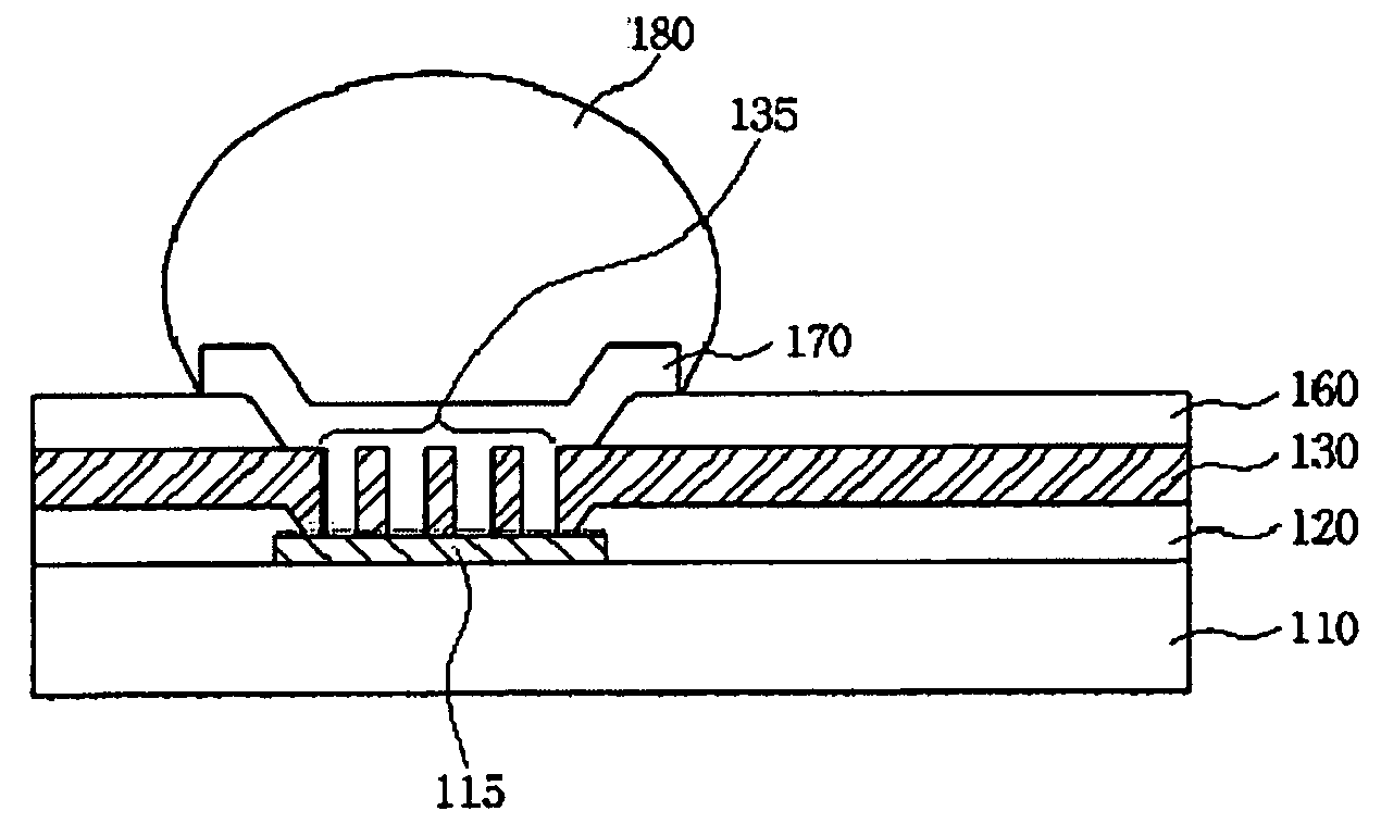
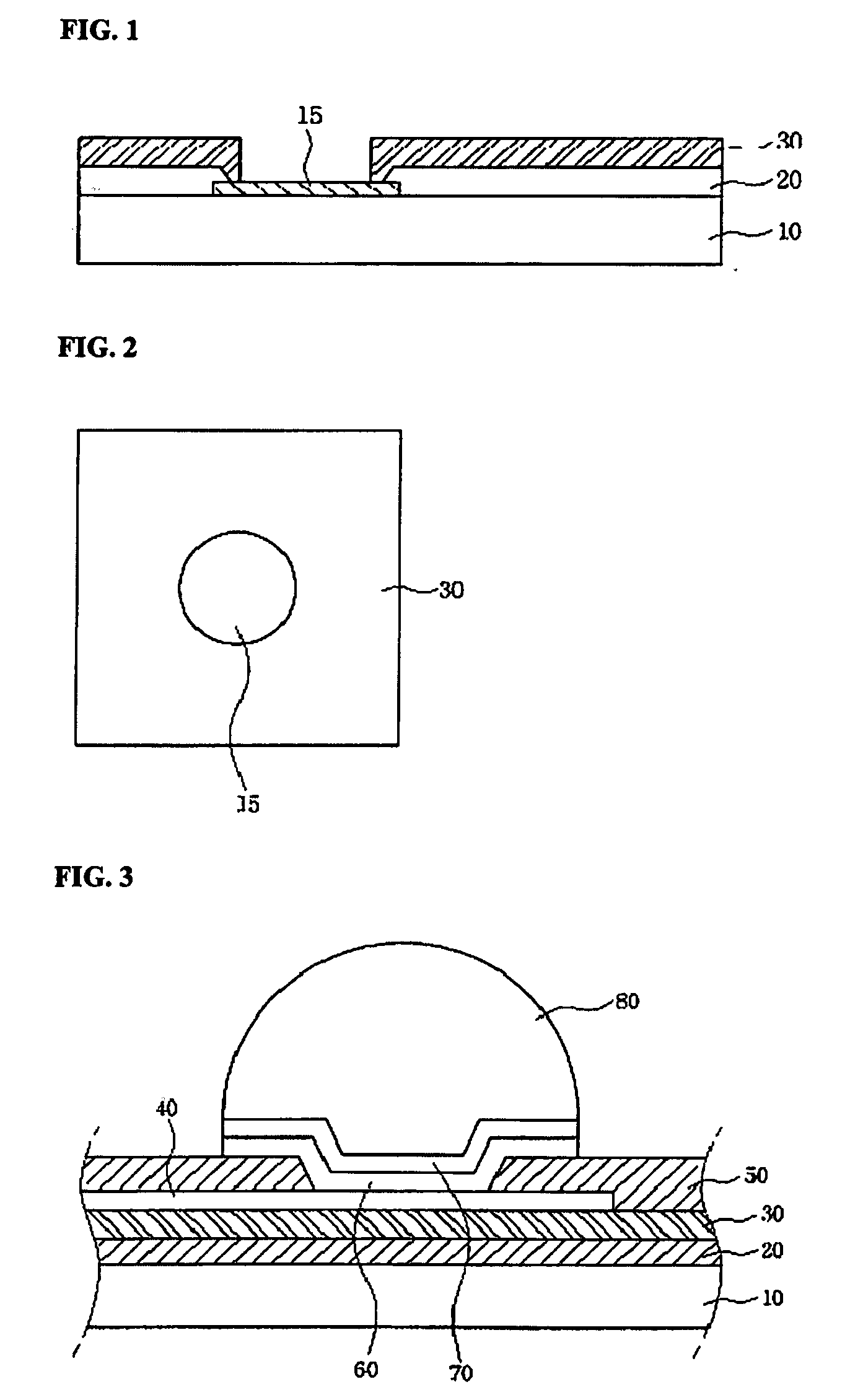
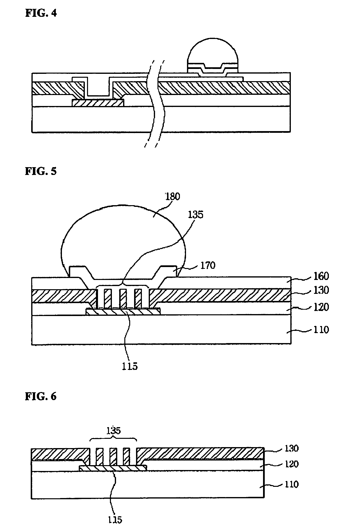
[0049]FIG. 5 is a sectional view illustrating a bump structure according to the present invention. As illustrated in FIG. 5, a substrate 110 including semiconductor devices is formed thereon with an electrode pad 115, the top surface of which is exposed by an insulating layer 120. The electrode pad 115 having the exposed top surface is formed thereon with a polymer layer 130. The polymer layer 130 includes a plurality of vias 135 on a region of the electrode pad 115. The vias 135 increase the surface area of an electrode while electrically contacting an UBM 170. Thus, current crowding is prevented, and current dispersion occurs, thereby improving the electrical properties of a semiconductor package. The top surface of the polymer layer 130 is formed thereon with another polymer layer 160 in order to relieve stress. The polymer layer 160 is exposed around the vias, and the exposed region of the polymer layer 160 is formed thereon with the UBM 170 and a metal bump 180.

second embodiment

[0050]FIG. 6 is a sectional view illustrating a redistributed structure of an electrode according to the present invention. A substrate 110 including semiconductor devices is formed thereon with at least one electrode pad 115, the top surface of which is exposed by an insulating layer 120. The electrode pad 115 having the exposed top surface is formed thereon with a polymer layer 130. The polymer layer 130 includes a plurality of vias 135 on a region of the electrode pad 115.

[0051]FIGS. 7 and 8 illustrate an example of a structure of a polymer layer 130 including a plurality of vias 135. Each via 135 may have various shapes such as a circular shape and a polygonal shape including a quadrangular shape. These vias 135 increase the surface area of a redistribution electrode (140 of FIG. 9), which extends from the electrode pad 115 and is redistributed. For example, when an electrode pad is formed to have one via having a radius of about 40 μm, and another electrode pad is formed to hav...


PUM


Abstract

A bump for a semiconductor package forms a polymer layer having multiple vias on an electrode pad above a semiconductor chip to increase an electrical contact area between the electrode pad and a metal bump. Further, the bump forms a polymer layer having multiple vias on a redistribution electrode pad to increase a surface area of an electrode interconnection. The multiple vias increase electrical and mechanical contact areas, thereby preventing current crowding and improving joint reliability. The bump for a semiconductor package may further comprise a stress relaxation layer at the lower portion of the bump.

Description

FIELD OF THE INVENTION[0001]The present inventions are directed to a bump for a semiconductor package, more particularly a bump with multiple vias and a method of fabricating the same.BACKGROUND OF THE INVENTION[0002]With high integration density, high performance and high-speed operation of semiconductor chips, much effort has been attempted to downsize and mass-produce semiconductor packages. For example, the semiconductor package has been proposed, which directly and electrically connects pads of a semiconductor chip and electrode terminals of a printed circuit board through bumps, which are made of solder or metal and formed on the pads of the semiconductor chip.[0003]A typical semiconductor package using the bump which is made of solder may be a flip chip ball grid array (FCBGA) package or a wafer level chip scale package (WLCSP). Meanwhile, a package using the bump which is made of metal may be a chip-on-glass (COG) package or a tape carrier package (TCP).[0004]The FCBGA packa...

Claims


Application Information

Patent Timeline
Patent Type & Authority Applications(United States)
IPC IPC(8): H01L23/488H01L21/60
CPCH01L24/03H01L2224/0231H01L24/11H01L24/13H01L2224/0401H01L2224/05557H01L2224/13006H01L2224/13007H01L2224/13022H01L2224/13024H01L2224/131H01L2224/13124H01L2224/13144H01L2224/13147H01L2224/16H01L2924/01013H01L2924/01014H01L2924/01022H01L2924/01025H01L2924/01027H01L2924/01028H01L2924/01029H01L2924/01047H01L2924/01049H01L2924/0105H01L2924/01075H01L2924/01078H01L2924/01079H01L2924/01082H01L2924/01322H01L2924/014H01L2924/10329H01L2924/19043H01L2924/30107H01L24/05H01L2224/0233H01L23/3192H01L2924/01019H01L2924/01023H01L2924/01024H01L2924/01033H01L2924/00014H01L2924/351H01L2224/1134H01L2224/05093H01L2924/00
Inventor PARK, YUN MOOK
Owner NEPES CO LTD
Why Eureka
Try Eureka